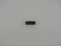
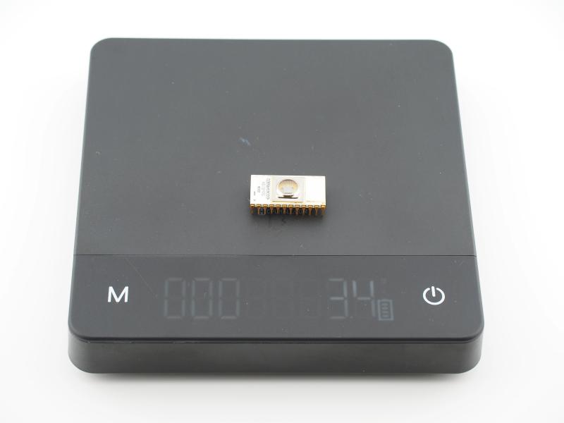
Dropping it on the scale, it weighs in at exactly 3.4 grams of pure Cold War paranoia and heavy metal engineering. The heavy gold brazing around the quartz window frame is a signature of high budget Soviet manufacturing.
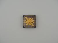
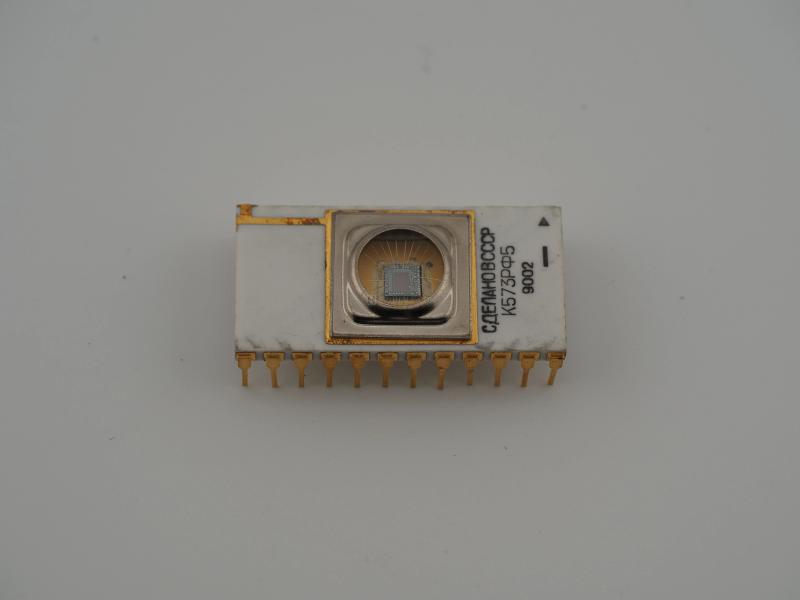
Front Surface Text:СДЕЛАНО В СССР
К573РФ5
9002
[Dash and Right-Pointing Triangle Mark]
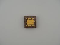
Back Surface Text:OX
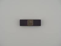
Looking at the bottom of this DIP package, the gold plated pins are remarkably pristine for a chip stamped in the second week of 1990. I also noticed a faint "OX" stamped in black ink on the underside.
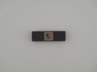
The surface text on the top is laser sharp. The Cyrillic "СДЕЛАНО В СССР" translates directly to "Made in USSR" and sits proudly above the part number and the date code. Off to the right, there is a distinct geometric horizontal dash next to a right pointing triangle. This is a classic and somewhat cryptic Soviet factory mark or orientation indicator. There is also a slight bit of oxidation or residual flux near the top left corner of the gold frame, hinting at the high heat processes used to seal the lid. Through that gorgeous optical quartz window, you can clearly see the silicon die and the microscopic gold wire bonds making their precarious jumps to the package lead frame.
Let us dive into the technical weeds. This is not a traditional processing unit but a dedicated memory block, specifically a 16 kilobit UV erasable EPROM organized as 2K by 8 bits. At the silicon level, this operates as a direct clone of the legendary Intel 2716. The silicon die utilizes NMOS technology and relies on floating gate transistors to store data persistently without power.
The quartz window is not just for our viewing pleasure. It is a strict functional requirement. To erase the chip, you have to blast that silicon die with intense ultraviolet light for about twenty minutes to excite the trapped electrons enough to escape the floating gates. Programming it required hitting the programming pin with a relatively massive 21 to 25 volts. The thermal challenges were negligible during read operations at a standard 5 volts, but the packaging complexity is off the charts. Sealing a piece of optical quartz into a ceramic and gold cavity while maintaining a perfect vacuum or inert gas environment requires serious metallurgical precision.
The drama surrounding this chip is the story of the Soviet Ministry of Electronic Industry. By the late 1970s, the USSR realized they were falling behind the American semiconductor juggernaut. Instead of designing entirely new architectures from scratch, they fired up a massive state sponsored reverse engineering machine. The Intel 2716 was a prime target. You cannot build a computer without ROM to hold the bootstrap code.
The K573RF5 became the lifeblood of Soviet computing, finding its way into cloned PDP-11 systems, early Agat microcomputers, and heavy industrial hardware. There is a persistent myth that the Soviets simply bought Intel chips, sanded down the logos, and rebranded them. Holding this piece proves that myth is absolutely false. They had to create their own fabrication lines, dope their own silicon wafers, and source their own ceramic packages. The physical engineering was entirely domestic, even if the logical architecture was lifted directly from Santa Clara. It is highly ironic to think that American operating codes likely ran natively on this deeply communist piece of silicon.
Placing this exact chip in the historical timeline requires reading the subtle clues on its surface. I can definitively state this is a commercial or industrial grade component because of the "K" prefix in the part number. Soviet military acceptance chips, known as "Fifth Acceptance", usually omitted the "K" and featured a prominent diamond stamp.
The "9002" date code places its birth in January 1990. This makes it a fascinating late era relic, manufactured just as the Soviet Union was beginning to physically and politically fracture. The physical build quality never faltered, though. The gold plating is as thick and lustrous as a chip made a decade prior. Identifying the exact fabrication plant is always a bit of a dark art with Soviet ICs. The geometric symbol on the lower right is sometimes attributed to specific manufacturing plants in Kiev or Zelenograd, but it also functioned as a standard Pin 1 orientation indicator for automated insertion machines. Whatever plant baked this ceramic, they did it with exceptional precision.