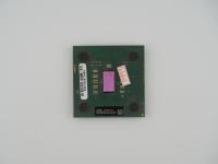
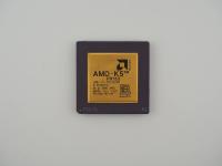
The sheer amount of information printed on the surface tells the entire story before I even look up the specs. This specific unit is built on the classic green Organic Pin Grid Array package.
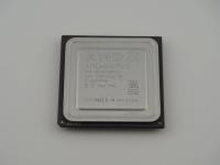
Examining the black label pad, the laser etching is remarkably legible:
AMD Sempron™
SDA2200DUT3D  Z486566K40793
BCXJB 0444GPMW  (M)(C) 1999 AMD
ASSEMBLED IN MALAYSIA
Warranty Sticker:CPI626391V15D122804/9
SEM 2200 15PC
TD43T25
Warranty Void if Removed
The date code 0444 confirms this silicon was minted in the 44th week of 2004. You can also clearly see the © 1999 AMD copyright, a nod to the foundational K7 architecture IP that powers this chip. Looking at the physical condition, the four circular foam crush pads in the corners have begun to dry out and crack. These pads were notoriously vital for stabilizing heavy coolers. Right next to the bare silicon die is a paper tag applied by a system integrator or local PC shop. The fact that a piece of paper survived years of heat cycling mere millimeters from a bare K7 die is a miracle in itself. The bare die exhibits a beautiful pinkish-purple reflection under studio lighting, showing off the raw silicon in all its fragile glory.
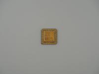
Breaking down the Official Part Number SDA2200DUT3D reveals the exact engineering parameters of this piece. The D indicates an OPGA package, U specifies a core voltage of 1.6V, and T tells us the maximum safe die temperature is a blistering 90 degrees Celsius. The 3 signifies 256KB of Level 2 cache, and finally, the D dictates a 333 MT/s Front Side Bus.
Underneath the hood, this is a Thoroughbred-B core manufactured on a 130-nanometer copper fabrication process. It packs approximately 37.5 million transistors into an incredibly tiny footprint. Unlike modern processors, this era of AMD silicon lacked an Integrated Heat Spreader. The cooler made direct contact with the fragile silicon die. If you mounted your heatsink at a slight angle, you risked chipping the corners of the die and instantly killing the processor. It was an era of hardware that demanded physical respect.
This chip represents a fascinating transition period for AMD. By 2004, the mighty Athlon XP line was stepping aside for the 64-bit K8 architecture. AMD needed a fresh brand to fight Intel's Celeron D in the budget sector, and the old "Duron" name carried too much baggage as a bottom-tier part. Enter the Sempron.
The most controversial part of the Sempron legacy is the Performance Rating system. This chip is branded as a "2200+", but it only operates at a physical clock speed of 1.5 GHz. AMD argued that clock speed alone was a flawed metric and claimed this chip performed equivalently to a 2.2 GHz Celeron. While technically true in many IPC-heavy workloads, the general public found the numbering scheme deeply confusing. It was a brilliant, albeit frustrating, piece of marketing warfare.
While I do not have the original purchase receipt for this specific unit, the physical clues leave no mystery about its past life. The paper sticker bearing SEM 2200 15PC and Warranty Void if Removed is a classic hallmark of early 2000s white-box system builders. These local shops would slap their own inventory tags directly onto the components before assembling cheap office towers for local businesses.
The stepping code BCXJB is well documented in vintage overclocking circles as a standard Thoroughbred-B variant. Some hardware enthusiasts mistakenly believe all early Semprons were based on the newer Thorton core, but the OPN and stepping here firmly prove this is a recycled Thoroughbred-B die. It almost certainly spent a decade running Windows XP and Microsoft Word in a dusty, poorly ventilated beige case before being rescued for the collection.