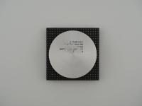
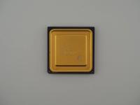
The contrast between the deep plum colored ceramic substrate and the massive gold heat spreader is a hallmark of 1990s heavy metal hardware.
This specific unit features two distinct circular mounting studs brazed directly onto the gold cap. These were used to secure massive, heavy heatsinks required to cool this beast. Examining the surface, the gold cap shows some very slight scuffing, but the laser etching on the ceramic remains incredibly sharp.
Here is the exact transcription of the surface markings:
SAMSUNG ELECTRONICS
GAKE17 804 0 (C) (M)

ALPHA(TM) 21164
KP21164-400CN   KKB   E56
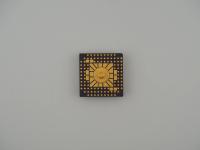
The gold pins on the underside are arranged in a staggered pattern. The braze points where the pins meet the ceramic are beautifully uniform, reflecting the high manufacturing standards required for enterprise grade silicon of this era.
The Alpha 21164 was an absolute monster of its time. While Intel was trying to convince the world that the Pentium Pro was the future of computing, Digital Equipment Corporation (DEC) was casually releasing processors that operated at nearly double the clockspeed of anything else on the market. This specific chip runs at 400 MHz. In the mid 1990s, that number was practically science fiction.
At its core, the 21164 (also known by its internal DEC codename EV5, or EV56 for later revisions) is a 64-bit RISC microprocessor. It features a superscalar in-order execution pipeline capable of issuing up to four instructions per clock cycle.
The real engineering magic of the 21164 was its memory hierarchy. It packed 9.3 million transistors, a massive count for the time. DEC achieved this by placing a 96 KB unified Level 2 cache directly on the processor die alongside the 8 KB instruction and 8 KB data L1 caches. Putting an L2 cache on die was extremely expensive and technically difficult, but it drastically reduced memory latency and allowed the chip to hit those blistering 400 MHz target speeds without starving for data. The chip also supported an enormous off-die L3 cache which was mounted directly on the motherboard.
The Alpha architecture is legendary among hardware enthusiasts. It represents an era when the performance crown was heavily contested and the x86 architecture was not the undisputed king of the server room. The Alpha was the speed demon.
What makes this specific artifact so interesting is the SAMSUNG ELECTRONICS branding. Why is a South Korean memory and electronics giant stamping their name on a proprietary DEC processor? The answer lies in fabrication limitations. As demand for Alpha processors grew, DEC realized their own fabrication plants could not produce the chips in high enough volumes or at the required yields for the newer, smaller process nodes. To solve this, DEC licensed the Alpha architecture and manufacturing rights to Samsung. Samsung had state of the art fabrication facilities and could pump out these 21164 chips reliably. Finding a Samsung branded Alpha is a fantastic piece of industry history because it perfectly illustrates the dawn of the fabless semiconductor model that dominates the industry today.
The ultimate tragedy of the Alpha architecture is well documented. Compaq bought DEC, then HP bought Compaq. HP systematically killed off the superior Alpha architecture to focus on Intel's ill fated Itanium project. Alpha died not because it was slow, but because of corporate consolidation and politics.
I am extremely confident in the identification of this piece. The surface markings leave no room for ambiguity. The KP21164-400CN part number explicitly confirms this is a Samsung fabricated Alpha 21164 designed to run at 400 MHz. The E56 marking on the bottom right is highly indicative of the EV56 core revision, which was a die shrink of the original EV5 down to a 0.35 micron process. This shrink was necessary to hit the 400 MHz clockspeed and added byte-word extensions to the instruction set.
The visual clues, from the exact pin layout of the SPGA-499 package to the proprietary heatsink mounting studs, perfectly match known engineering samples and production units of the Samsung licensed Alpha 21164 line.