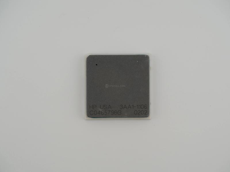
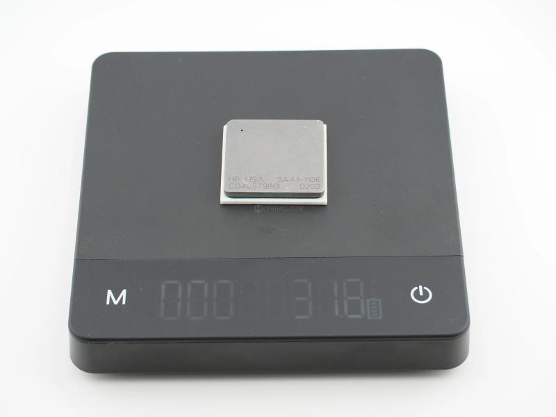
Holding this piece in my hand, the very first thing I notice is the sheer density. As verified by the scale in our documentation, this surprisingly compact square weighs in at a hefty 31.8 grams. It feels less like a modern processor and more like a solid block of industrial shielding.
The surface text is laser-etched directly into the dark grey heat spreader, faint but perfectly legible under macro lighting:
HP USA      3AA1-1106
C0465796G       0202
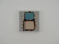
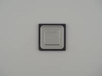
Flipping the artifact over reveals a mesmerizing, pristine array of gold pads. This is a classic Land Grid Array package, but the pads themselves are incredibly robust, completely lacking the delicate pins of consumer chips from the same era.
The side profile is where the engineering truly shows off. It presents a beautiful layered construction. On top, we have the thick, dark grey metallic lid. Just below that sits a thin blueish-green substrate material, which is finally bonded to a thick, brilliantly white ceramic base. Etched right along the side edge of the white ceramic is a secondary serial or batch identifier:
C0465796G-192
The 0202 date code heavily implies this unit was stamped in the second week of 2002. This places it perfectly in the transition window between the standard PA-8700 and the slightly faster PA-8700+ silicon.
The internal architecture of this chip is nothing short of spectacular for its time. Built on a 0.18-micron Silicon-on-Insulator (SOI) process, the PA-8700 was a massive brute-force approach to data processing.
Most processors of this era relied on a small chunk of fast L1 cache and a larger, slower L2 cache to keep the pipeline fed. HP engineers decided to throw out the rulebook. They crammed an absolutely staggering 2.25 Megabytes of high-speed SRAM directly onto the die to serve as the L1 cache (split into 0.75MB for instructions and 1.5MB for data). Because this massive pool of memory operated at the full core clockspeed, the PA-8700 did not even need an L2 cache.
This design choice made the die absolutely massive, consuming around 144 million transistors. Pushing this much high-speed cache on a single piece of silicon generated significant thermal load, perfectly explaining the need for the thick ceramic base and the incredibly heavy heat spreader we see physically bonded to the top. This chip was designed to power massive, multi-processor HP Superdome servers, meaning thermal stability across dozens of clustered processors was an absolute requirement.
The history of the PA-8700 is deeply rooted in corporate survival and internal hardware drama. At the turn of the millennium, HP had publicly bet its future on the Itanium architecture, a joint venture with Intel that was supposed to completely replace RISC designs.
However, Itanium suffered from brutal delays and underwhelming initial performance. HP enterprise customers, running massive banking databases and telecommunications grids on HP-UX, were getting nervous. Sun Microsystems was attacking them with UltraSPARC, and IBM was pushing POWER hard.
The PA-8700 was essentially HP's fail-safe mechanism. It was proof that the older PA-RISC instruction set, when combined with a monstrous cache and clever fabrication, could still deliver devastatingly fast integer performance. It kept HP's server business highly profitable while the rest of the company waited for Itanium to become viable. There is an enduring myth among vintage server admins that HP engineers intentionally sandbagged some PA-RISC development to make Itanium look better, but chips like this artifact prove the exact opposite. They pushed the silicon to its absolute physical limits.
Confirming the exact stepping of HP proprietary silicon can be a forensic challenge because HP utilized internal part numbers rather than public marketing names on the die covers.
The primary identifier C0465796G is a classic HP manufacturing code for their high-end server components. By cross-referencing the heavy square LGA form factor with the 0202 date code, we can decisively rule out older PGA chips like the PA-8500 or PA-8600. The PA-8800 "Mako" chips that followed utilized dual-core multi-chip modules that look fundamentally different from this single monolithic spreader.
Therefore, I am highly confident this is a PA-8700 series processor. Given the 2002 timestamp, it is very likely the PA-8700+ revision, which saw the clockspeed bumped up to 875 MHz to squeeze out just a little more performance before the next generation arrived. It remains a beautiful, heavy testament to the golden age of proprietary Unix hardware.