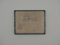
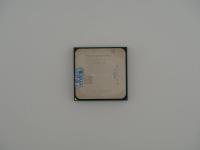
Placing this specific unit on the scale, it registers a satisfying 30.9 grams. It has that dense, utilitarian feel typical of enterprise hardware. The integrated heat spreader dominates the top, featuring a matte metallic finish that contrasts perfectly with the crisp laser etching.
Here is the exact surface transcription from the heat spreader:
AMD Opteron™
OS4170OFU6DGO
CCAID CA 1146PGT
4183834H20085
AMD (logo) (c) 2009 AMD
DIFFUSED IN GERMANY
MADE IN MALAYSIA
30602                    C
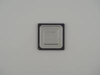
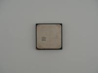
Turning the artifact over reveals a stunning expanse of 1207 flat gold contact pads. Unlike the consumer chips of the era that still bristled with delicate pins, this server part utilizes a Land Grid Array. The pads are arranged in a massive rectangular block with specific corner keying to prevent catastrophic insertion errors into the socket. The fiberglass substrate feels incredibly rigid, an absolute necessity to withstand the immense mounting pressure required by enterprise server heatsinks.
This silicon is built around the "Lisbon" core, part of the mature 45 nanometer Silicon-on-Insulator manufacturing process churned out by GlobalFoundries in Dresden. Underneath that heavy metal lid sits a native six-core die. AMD was heavily pushing the concept of "true" multi-core processors at the time, contrasting their monolithic designs against some of Intel's multi-chip module approaches from earlier generations.
The engineering marvel here is hidden in the "HE" suffix of its marketing name, which stands for Highly Efficient. The K10 architecture could be notoriously power hungry at higher clocks. By dropping the clockspeed to a modest 2.1 GHz, AMD engineers managed to squeeze six physical cores into a remarkably tight 50W Thermal Design Power envelope. This was a critical achievement for high-density 1U and 2U rackmount servers where cooling overhead directly translated to datacenter operational costs. The chip also features 6MB of shared L3 cache and supports dual-channel DDR3 memory, pushing data through AMD's proprietary HyperTransport 3.0 links to ensure bottlenecks were kept to an absolute minimum.
The Opteron 4100 series, codenamed "San Marino" for the platform and "Lisbon" for the processor, arrived at a bizarre transitional period for AMD. The tech world was just starting to obsess over "The Cloud." Datacenter managers were demanding dense, low-power nodes to handle highly parallel but relatively lightweight web-serving tasks. This processor was AMD's direct answer to Intel's low-power Xeon L-series.
The lore surrounding this era of AMD is bittersweet. The K10 architecture was aging. It was solid, reliable, and fundamentally sound, but it lacked the brutal per-core IPC advantage that Intel commanded with their Nehalem and Westmere architectures. As a result, AMD competed fiercely on price and power efficiency. This specific chip represents the calm before the storm. It was one of the last pure K10 server chips deployed before AMD launched the infamous "Bulldozer" architecture. Bulldozer would ultimately drag AMD through years of enterprise market share losses. Therefore, collectors and enthusiasts often look back at these six-core Lisbon chips as the reliable, sensible workhorses of a bygone era.
Identifying this artifact requires breaking down AMD's strict Ordering Part Number system. The string OS4170OFU6DGO tells us exactly what we hold.
The "OS" signifies Opteron Server. The "4170" dictates the model number. The "OF" is the critical power indicator, translating to the 50W TDP limit. The "U" denotes the physical Socket C32 interface. The "6" confirms the six physical cores. Finally, the "D" points to the 6MB L3 cache and the "GO" identifies the specific D1 stepping of the Lisbon silicon.
Furthermore, the secondary line CCAID CA 1146PGT gives us the exact birthdate of this specific unit. The "1146" indicates it was packaged in the 46th week of 2011. This puts its manufacture date well into the lifespan of the platform, likely fulfilling a large enterprise contract for a web hosting provider scaling up their infrastructure. The silicon itself was etched in Germany, while the final assembly and testing occurred at AMD's facilities in Malaysia.