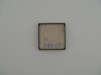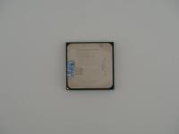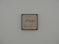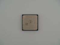

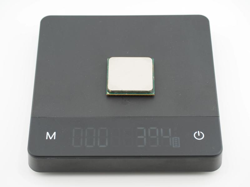
Dropping it onto the testing scale, it weighs in at exactly 39.4 grams. This is typical for a modern lidded desktop processor where the bulk of the mass comes from the stamped copper Integrated Heat Spreader (IHS) and the thermal interface material beneath it.
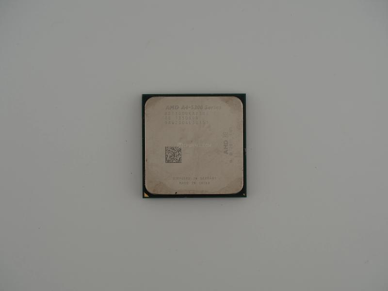
The laser-etched typography on the heat spreader is highly legible and provides a complete map of this chip's identity.
AMD A4-5300 Series
AD5300OKA23HJ
GB 1350SUN
9AW2004L30151
(c) 2011 AMD
DIFFUSED IN GERMANY
MADE IN CHINA
Looking at the back of the fiberglass substrate, the layout is classic Socket FM2. The gold-plated pins form a dense grid, completely surrounding a small central cavity. That pin-free center island is populated by microscopic surface-mount capacitors responsible for smoothing out power delivery to the die. The pins themselves show minor signs of handling but remain uniformly straight. The "Diffused in Germany" text confirms the silicon wafer was baked at GlobalFoundries Fab 1 in Dresden before being shipped to China for packaging and final assembly. The date code 1350SUN tells me exactly when this specific chip was born: the 50th week of 2013.
Beneath the metal lid lies the "Trinity" silicon die. Built on GlobalFoundries' 32-nanometer Silicon-on-Insulator (SOI) process, this chip is fundamentally a marriage of AMD's Piledriver CPU architecture and their TeraScale 3 graphics architecture.
The A4-5300 features a single Piledriver module. Because of AMD's highly controversial design choices during this era, a single module contains two integer clusters but shares a single floating-point unit (FPU). AMD marketed this as a "dual-core" processor, a semantic decision that would later result in class-action lawsuits for their higher-end FX chips. It runs at a base clock of 3.4 GHz and can boost up to 3.6 GHz, operating within a very manageable 65-watt thermal design power (TDP).
The true engineering focus of this chip was the integrated graphics. The on-board Radeon HD 7480D occupies a significant portion of the silicon die. It features 128 Radeon cores running at 724 MHz. While those specs look microscopic by today's standards, integrating a fully functional DirectX 11 capable GPU onto the same die as the CPU was a massive feat of engineering at the time, completely eliminating the need for a discrete graphics card in budget systems.
This artifact represents a fascinating era of survival for AMD. In the early 2010s, Intel's "Core" architecture was absolutely dominating the high-end desktop market. AMD's Bulldozer architecture had failed to capture the performance crown. To stay alive, AMD leaned heavily into their acquisition of ATI Technologies and pushed the "Fusion" concept. The goal was to build Accelerated Processing Units (APUs) that offered "good enough" CPU performance paired with integrated graphics that absolutely destroyed Intel's onboard video.
The A4-5300 was the bottom tier of this strategy. This chip powered countless office PCs, basic media centers, and computers built for grandparents. It was never meant to break benchmarking records. It was meant to be cheap, reliable, and capable of rendering Windows 7 and 1080p YouTube videos without a dedicated graphics card.
There is an old enthusiast joke that these early APUs were basically just GPUs with a tiny CPU strapped to their back to feed them data. While structurally untrue, it perfectly captures the design philosophy. The heavy lifting in this silicon architecture was done by the Radeon graphics block. Chips exactly like this one paid the bills and kept the lights on at AMD headquarters just long enough for their engineers to secretly develop the Ryzen architecture that would eventually save the company.
Identifying this artifact requires zero guesswork. The factory laser etching provides an explicit Ordering Part Number (OPN): AD5300OKA23HJ.
Decoding this alphanumeric string reveals the exact specifications. The A stands for the AMD A-Series. The D denotes Desktop. The 5300 is the model number. The O indicates a 65W TDP class. The K specifies the Socket FM2 package. The A2 points to the cache configuration. The 3 dictates the dual-core nature, and the HJ signifies the specific stepping revision of the silicon. Everything aligns perfectly with the visual evidence of the physical package and the weight. I am looking at a textbook example of a Trinity-era APU.