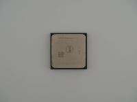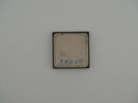
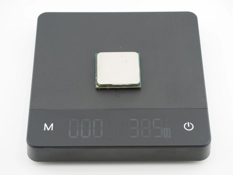
It weighs exactly 38.5 grams. That is a solid, satisfying chunk of fiberglass, copper, and silicon. This specific artifact is an AMD FX-4300, a budget entry from one of the most hotly debated eras in modern computing history.
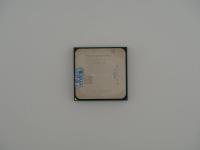
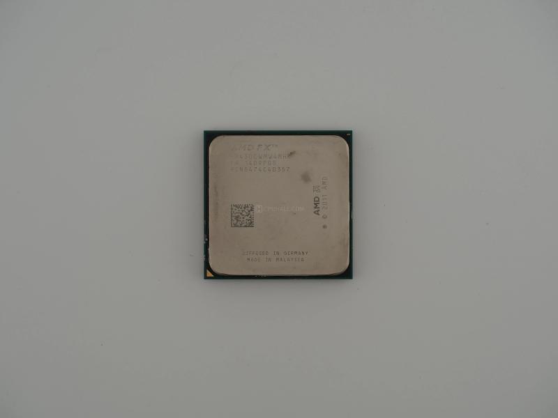
Here is the exact surface transcription from the heat spreader:
AMD FX™
FD4300WMW4MHK
FA 1409PGS
9CN8474C40357
AMD (logo) (C) 2011 AMD
DIFFUSED IN GERMANY
MADE IN MALAYSIA
Flipping it over reveals the classic Pin Grid Array. The golden forest of 942 pins is pristine on this specimen. None are bent. I always appreciate the tactile feel of these AM3+ chips. The gold against the dark green organic substrate is the quintessential look of early 2010s desktop computing. It lacks the exotic ceramic and heavy gold caps of the mainframe era, but it has an undeniable industrial charm.
This processor represents the "Vishera" die, which utilized the Piledriver microarchitecture. Piledriver was the highly necessary refinement to the original, infamous Bulldozer architecture. Fabricated on a 32 nanometer Silicon-on-Insulator process by GlobalFoundries in Dresden, Germany, this chip had a lot of heavy lifting to do.
The engineering approach here was highly unconventional at the time. The FX-4300 operates with a base clockspeed of 3.8 GHz and a turbo frequency of 4.0 GHz. It carries a Thermal Design Power of 95 Watts. While 95W seems tame compared to the terrifying 220W FX-9590 that came from the same silicon lineage, it was still quite power-hungry for a budget processor.
The core layout is where the deep technical fascination lies. AMD marketed this as a quad-core processor. Inside the silicon, there are two "Piledriver Modules". Each module contains two integer clusters but only one shared Floating Point Unit. It features 4MB of L2 cache and 4MB of shared L3 cache. The decision to share resources between integer cores to save die space and increase thread count ultimately defined the entire performance profile of this processor generation.
You cannot look at an FX series chip without talking about the lore. The Bulldozer and Piledriver families are legendary, though perhaps not for the reasons AMD originally intended. When this chip launched, the desktop market was locked in a brutal frequency and core count war. AMD bet the farm on highly multithreaded workloads becoming the immediate industry standard.
They gambled heavily. They lost.
Because each dual-core module shared a single FPU and instruction fetch/decode stage, single-threaded performance suffered terribly compared to Intel's competing Sandy Bridge and Ivy Bridge architectures. If you were playing games in 2012, single-core speed was king. The FX chips notoriously bottlenecked high-end graphics cards.
However, the real historical weight of this artifact comes from the courtroom. The unique shared-resource architecture led to a massive class-action lawsuit. Consumers argued that because the "cores" shared vital components, chips like the FX-8350 and this FX-4300 were not true eight-core or quad-core processors. AMD eventually settled the lawsuit in 2019. It is incredibly rare that CPU microarchitecture definitions end up being argued in front of a judge. That legal drama makes these chips a fascinating piece of tech history.
Verifying this chip requires no guesswork. The markings are definitive and tell a complete story of its origin.
The primary Ordering Part Number on the lid is FD4300WMW4MHK. Breaking down this string reveals everything we need to know. FD stands for FX Desktop. 4300 is the specific model number. The WM denotes the 95W AM3+ package. W4 confirms the physical presence of 4 active integer cores. Finally, the MHK suffix is the goldmine. It identifies the silicon stepping as C0, confirming it as the Piledriver-based Vishera die rather than older Zambezi silicon.
The date code reads 1409. This tells me this specific unit was packaged in the 9th week of 2014. By early 2014, the Vishera architecture was already fully mature, and AMD was producing these in massive quantities to serve the budget builder market. The "Diffused in Germany" and "Made in Malaysia" lines perfectly track with AMD's supply chain at the time. GlobalFoundries Fab 1 in Dresden handled the complex 32nm silicon wafer fabrication, and the bare dies were shipped to Penang, Malaysia for final mounting and pin-grid packaging.
It may not be the fastest chip in the museum, but it is a perfect physical representation of the lessons the industry had to learn before the modern Ryzen era could be born.