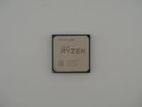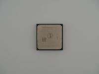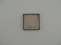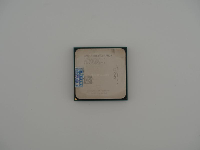

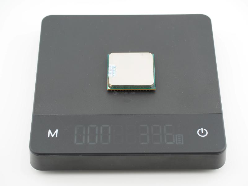
Dropping it onto the scale, it clocks in at exactly 39.6 grams. The thick integrated heat spreader dominates the top, bearing the battle scars of a few clumsy heatsink mounts and a torn blue holographic distributor seal. That sticker is a dead giveaway of this chip's life cycle. It tells me this processor spent its life circulating through the Asian grey market or as a bulk tray pull from an old prebuilt system, rather than arriving in a pristine retail box.
AMD Athlon™ X4 FM2+
AD830XYBI44JA
JB 1626SUS
9GP4354G60738
AMD (logo) (c) 2013 AMD
DIFFUSED IN GERMANY
MADE IN CHINA
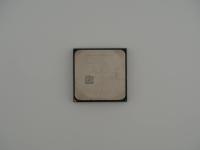
Flipping it over to inspect the underside, we have the classic Socket FM2+ 906-pin layout. The pins are remarkably straight for a tray-handled chip. The substrate itself is a standard green fiberglass weave, and the laser etching on the lid is still sharp, calling out the 2013 copyright date of the package design, even though the silicon inside was baked significantly later.
Diving into the weeds of this silicon reveals exactly what AMD was doing to stay afloat in the mid 2010s. This is a Kaveri die, built on the 28-nanometer SHP (Super High Performance) node by GlobalFoundries in Dresden, Germany. However, you will notice there are no "Radeon" markings anywhere on this package. That is because the Athlon X4 line from this era consists of "harvested" APUs.
AMD manufactured these chips intending for them to be A-Series APUs with integrated GCN graphics. When a chip came off the wafer with defective graphics cores, instead of throwing it in the trash, AMD simply laser-fused the GPU section off and sold the remaining functional CPU cores as an Athlon X4.
Underneath the hood, this chip utilizes the Steamroller microarchitecture. It features two modules, which house four integer clusters and two floating-point units. It is a 65W TDP part, meaning it ran relatively cool compared to the fire-breathing 95W variants in the same family. The base clock sits at a modest 3.0 GHz. It is a masterclass in recycling imperfect silicon to fill a budget market segment.
This artifact belongs to the infamous "Construction Core" era of AMD. We are talking about the long, painful lineage of Bulldozer, Piledriver, Steamroller, and Excavator. For PC builders, this era is mostly remembered as a time when Intel's Core series dominated the high end and AMD was forced into a price war at the absolute bottom of the barrel.
While the Athlon X4 860K is a legendary budget overclocker from this exact same family, the X4 830 we have here is its obscure, locked-down sibling. It was almost exclusively an OEM part, shipped in massive quantities to companies like HP and Lenovo to hit a specific price point for big box store desktops.
The great myth of this era is that these chips were "true" quad cores. A massive class-action lawsuit actually targeted AMD over this exact architectural choice. Because two integer cores shared a single floating-point unit within a module, performance heavily bottlenecked in certain workloads. History has not been kind to the Steamroller architecture, but pieces like this kept AMD financially breathing long enough to develop the Ryzen architecture that would eventually save the company.
Identifying this exact model requires a forensic breakdown of the OPN code: AD830XYBI44JA.
I can read this string like a book. The AD dictates it is an AMD Desktop processor. The 830X confirms the exact model number. The YB designation is crucial as it identifies the 65-watt thermal envelope. The I indicates the Socket FM2+ package. The two 4s represent four logical cores and 4MB of L2 cache. Finally, the JA suffix is the definitive signature of the Kaveri die revision.
What I find incredibly fascinating about this specific unit is the date code: 1626. This means the chip was packaged in the 26th week of 2016. AMD originally launched the Kaveri architecture back in early 2014. The fact that they were still pumping out these budget 28nm silicon wafers in mid-2016 highlights just how desperate the company was to maintain volume shipments right up until the final months before the Zen launch. This chip is a survivor from the very end of an architectural dead end.