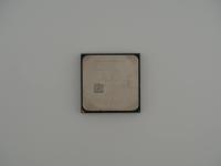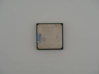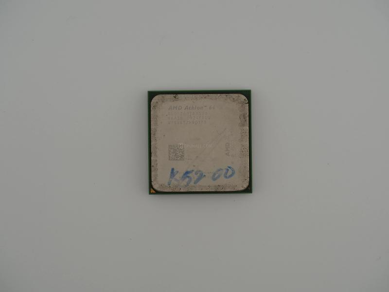
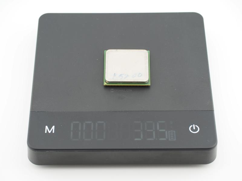
Dropping this piece on the scale reveals a solid 39.5 grams of classic desktop silicon. Holding this specific unit in my hand takes me right back to the trenches of the mid-2000s core wars. The visual condition of the Integrated Heat Spreader is thoroughly heavily used. Someone at a surplus recycler clearly took a blue marker and scribbled K5200 right across the metal, permanently branding it with its own model number.
Looking closely at the laser etching, the precise part numbers become visible through the grime.
AMD Athlon 64 X2
ADO5200IAA5DO
NAAIG 0924FPEW
W754452F90173
DIFFUSED IN GERMANY
MADE IN MALAYSIA
(m) (c) 2005 AMD
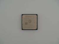
Flipping it over exposes the sea of 940 gold-plated pins protruding from the green organic substrate. The pins are entirely intact and remarkably straight. The standard Socket AM2 keying is visible in the corners where the pin grid is intentionally left blank.
The part number ADO5200IAA5DO is a complete technical map if you know how to decode AMD's ordering strings from this era. This is not just any 5200+. The ADO prefix marks this specifically as a 65-watt "Energy Efficient" variant. Standard early Athlon 64 X2 chips ran terrifyingly hot and drew up to 89W or even 110W. AMD desperately needed to tame their thermals.
The crucial detail here is the DO suffix at the end of the first line. That two-letter code identifies the silicon die underneath the lid as the Brisbane core. Moving away from the older 90nm Windsor cores, Brisbane was AMD's pivotal shift to a 65nm fabrication process. It features 512KB of L2 cache per core (indicated by the 5 in the OPN) and runs at a respectable 2.7 GHz.
Because this is a Socket AM2 chip, it carries one of AMD's most brilliant architectural advantages of the era. The memory controller is integrated directly onto the CPU die itself rather than sitting on a separate motherboard Northbridge. Socket AM2 specifically upgraded this integrated controller to support dual-channel DDR2 memory, completely eliminating the memory bottlenecks that plagued older systems.
The Athlon 64 X2 family absolutely humiliated Intel when it first dropped. While Intel was trying to glue two scalding-hot Pentium 4 NetBurst dies together to create the disastrous Pentium D, AMD had designed the K8 architecture from the ground up for native dual-core execution. It was a masterpiece of processor design.
However, by the time this specific Brisbane 5200+ hit the market, the tables had violently turned. Intel had unleashed the legendary Core 2 Duo architecture, reclaiming the performance crown with ruthless efficiency. The Brisbane cores became AMD's defensive line. They could not beat Intel's flagship chips in raw speed, so AMD pivoted to fighting a vicious price war. This chip was a budget warrior. It provided incredibly cheap, reasonably cool dual-core performance for the masses.
There is a funny historical quirk about the Brisbane cores. AMD used fractional clock multipliers to hit specific frequencies on these chips. Because the memory controller derived its speed from the CPU core clock divided by an integer, Brisbane CPUs often ran their DDR2 memory at slightly lower frequencies than officially advertised. You would buy DDR2-800, but your 2.7 GHz Brisbane would force it to run at 771 MHz. Hardware forum purists used to lose their minds over this microscopic loss of bandwidth.
There is no mystery regarding the identity of this artifact. The laser markings are definitive and align perfectly with standard AMD documentation. What makes this specific artifact fascinating to me is the date code: 0924.
This tells us the chip was manufactured in the 24th week of 2009. That is shockingly late for a Socket AM2 K8 processor. By mid-2009, AMD had already launched the Phenom II architecture and the newer Socket AM3 platform. The fact that AMD was still stamping out these 65nm Brisbane chips in 2009 proves just how lucrative the low-end, budget replacement market was. This chip was likely destined for a basic office pre-built machine or an exceptionally cheap motherboard bundle. The blue marker scrawl on the front suggests it was eventually pulled from an aging corporate tower, tossed in a bin of recycled parts, and graded strictly by its model number for quick resale.