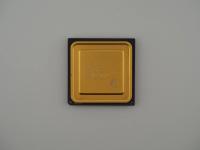
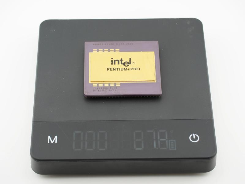
This is not just a processor. It is a brick of computing history. Dropping it on my digital scale registers a hefty 87.8 grams. That is a massive amount of dark purple ceramic and gold-plated tungsten.
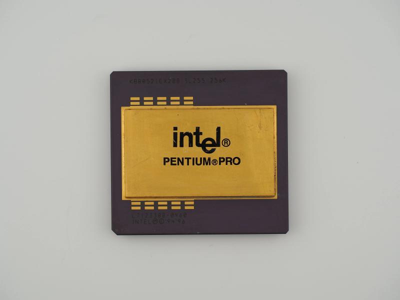
Here is the exact surface transcription from the top of the ceramic substrate and the gold heat spreader:
KB80521EX200 SL255 256K
intel (R) PENTIUM (R) PRO
L7123388-0460
INTEL (M)(C) '94 '96
Flipping the heavy ceramic slab over reveals the dual-cavity layout hidden beneath a black central resin block, surrounded by hundreds of beautifully brazed gold pins. The laser etching on the bottom reads:
17024910AB
MALAY
KB80521EX200
SL255 256K
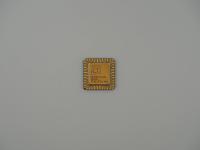
Holding this piece, I immediately notice the absolute rigidity of the SPGA-387 package. The gold heat spreader is cold to the touch and bears a few micro-scratches from decades of handling, which only adds to its industrial charm. The deep plum hue of the ceramic provides a gorgeous contrast against the polished gold pins. Before I place this back into the 125L digital dry cabinet to sit comfortably at 40% humidity, we need to appreciate what is happening inside this heavy metal sandwich.
The Pentium Pro is an absolute marvel of 1990s packaging technology. What we are looking at is not a single piece of silicon. This is a Multi-Chip Module (MCM). Intel placed the primary CPU die and a massive secondary L2 cache die on the same package, connecting them with a high-speed, backside bus via thousands of microscopic wire bonds.
This specific SL255 stepping runs at 200 MHz and features a 256KB L2 cache. While 256KB sounds tiny today, the cache die actually had significantly more transistors (15.5 million) than the CPU die itself (5.5 million). Manufacturing this was a nightmare for Intel. Because both dies were permanently bonded to the package before final testing, a flaw in either the CPU or the cache meant the entire expensive assembly had to be thrown in the trash. Yields were initially brutal.
Built on a 0.35-micron BiCMOS process, this chip ran incredibly hot for its era. That massive gold-plated tungsten slab on top is not there for vanity. It is a critical thermal conduction pathway needed to bleed heat away from the dual dies, a design philosophy that reminds me slightly of the thermal management strategies used in large-scale IBM modules.
The P6 architecture introduced by the Pentium Pro is arguably the most important foundation in Intel's history. This architecture introduced out-of-order execution, speculative execution, and the concept of a micro-op translation engine to the x86 world.
However, the Pentium Pro is also famous for a spectacular market quirk. It was aggressively optimized for 32-bit code, specifically for operating systems like Windows NT or UNIX. When normal consumers bought this incredibly expensive chip to run Windows 95, they were met with a nasty surprise. Windows 95 still relied heavily on legacy 16-bit code, which caused massive pipeline stalls in the P6 architecture. A much cheaper Pentium Classic could often outpace a Pentium Pro in 16-bit applications.
It gained a reputation as a consumer flop, but it absolutely dominated the enterprise server space. More importantly, the core P6 design was so robust that Intel simply added MMX instructions, moved the cache off the primary package to improve yields, and rebranded it as the Pentium II. The DNA of this exact chip powered Intel processors all the way through the Core architecture dominance.
There is no mystery regarding the identity of this artifact. The laser etchings provide complete, authoritative provenance. The KB80521EX200 part number confirms it is a 200 MHz part, and the SL255 S-Spec is a perfectly documented retail and OEM stepping.
The date code L712 tells a very specific origin story. The L indicates fabrication in Malaysia, the 7 stands for the year 1997, and the 12 means it rolled off the assembly line during the 12th week of that year. Even though the architecture launched in late 1995, this particular unit was manufactured right as the Pentium Pro was reaching its mature production peak, right before the Pentium II took over the spotlight. It is a pristine example of server-grade silicon from the golden era of heavy ceramic computing.