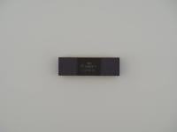
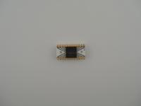
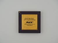
Here we have a remarkable slice of Cold War engineering. The scale puts it precisely at 3.2 grams, and the heavy white ceramic package feels practically bulletproof. This specific unit features a side-brazed 24-pin layout with thick, lustrous gold plating on the pins and traces that wrap around the substrate.
The top of the chip is dominated by a quartz window intended for UV erasure, exposing the beautiful silicon die beneath. Surrounding the window is a thick, amber-colored epoxy or glass frit seal that gives the piece an incredibly raw, industrial aesthetic. Looking closely at the top face, I can read the following markings:
(Oval with a '3' or 'Э' logo)
К573РФ1
8505
There is also a crude '4' or perhaps a Cyrillic 'Ц' hand-written in black marker near the bottom edge of the top ceramic plate. The underside of the chip is relatively barren save for a very faint stamped '17'. The visual contrast between the stark white ceramic, the rich gold pins, and the crude hand-markings makes this piece a stunning display of Soviet manufacturing sensibilities.
Diving into the technical weeds, the К573РФ1 is an ultraviolet-erasable programmable read-only memory chip (EPROM). It holds a staggering one kilobyte of data, organized as 1024 words of 8 bits each. To erase whatever code is trapped inside this floating-gate memory, you have to expose that quartz window to high-intensity 253.7 nm ultraviolet light for about twenty to thirty minutes.
This piece operates on N-channel MOS (NMOS) technology. Modern hardware enthusiasts are spoiled by simple single-voltage components, but firing up this artifact requires a very specific and unforgiving power delivery system. You must supply it with +12V, +5V, and -5V rails. If you sequence these voltages incorrectly or drop the -5V substrate bias, you will instantly destroy the chip. The programming process itself requires throwing a +26V pulse at the chip to force electrons into the floating gates. It is a hostile, high-voltage beast that requires extreme respect on the bench.
The history of Soviet microelectronics is heavily defined by a massive, state-sponsored effort to reverse-engineer Western silicon. The К573РФ1 is a direct, unapologetic clone of the legendary Intel 2708 EPROM. During the technology embargoes of the Cold War, the USSR could not legitimately purchase advanced integrated circuits for their military or industrial sectors. Instead, they acquired Western chips through covert channels, decapped them, and laboriously traced the lithography masks by hand to produce their own domestic variants.
This architecture was absolutely vital. Before the widespread availability of reliable magnetic storage or EEPROMs, these UV-erasable chips were the only practical way to hold bootloader code, BIOS ROMs, or critical constants for Soviet mainframes and early microcomputers like the Radio-86RK. You will find these chips heavily utilized in Soviet military hardware, industrial CNC machines, and aerospace applications. The thick ceramic and heavy gold plating on my unit perfectly reflect the "built for a tank" mentality of Soviet state electronics.
When I cross-reference the markings on this specific unit with my archives, the identification is rock solid. The К573РФ1 part number perfectly matches the Soviet designation for their Intel 2708 equivalent. The date code 8505 indicates this specific piece of silicon was manufactured in the fifth week of 1985.
The logo in the upper left corner, an oval enclosing a stylized '3' or Cyrillic 'Э', points to one of the many state-owned semiconductor plants distributed across the USSR. While tracking down the exact factory for every Soviet clone can be a maze of rebranded military plants, this specific mark is highly characteristic of the era. The lack of a distinct diamond stamp (which typically denotes the highest military 'VP' acceptance grade) suggests this might have been destined for high-end industrial, scientific, or domestic computing use rather than a missile guidance system. However, the sheer volume of gold used in the side-brazing indicates a budget far exceeding typical commercial electronics of the 1980s. It is a brilliant, heavy metal survivor from behind the Iron Curtain.