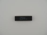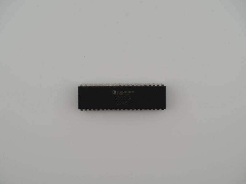
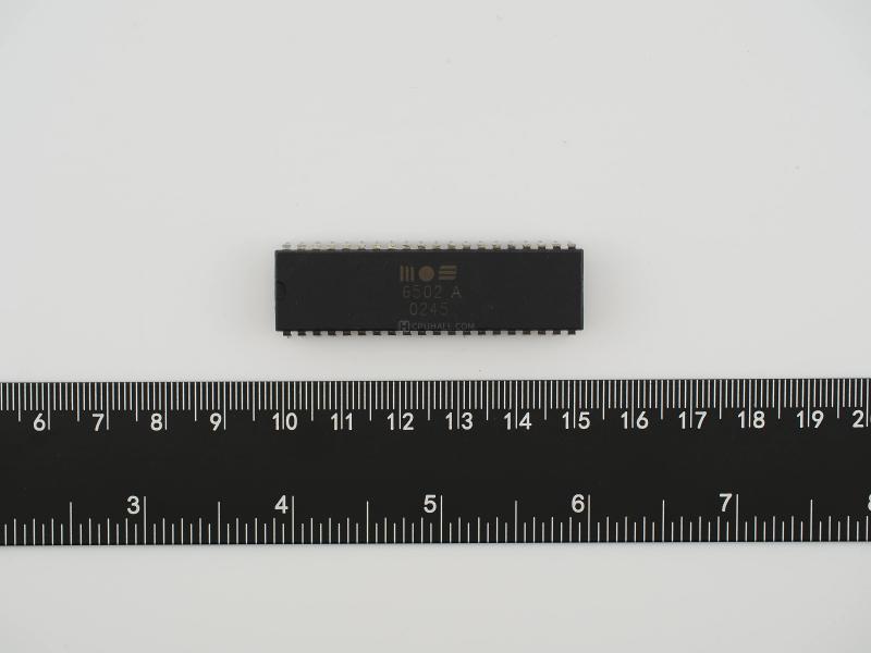
Clocking in at exactly 5.9 grams on the scale, this specific unit is a masterclass in minimalist 1970s packaging. It measures roughly 50 millimeters across its length, housed in a standard, slightly textured black plastic Dual In-line Package.
When you get up close, the matte surface of the plastic reveals a very subtle, almost porous grain. The pins have dulled over the decades, shifting from their original bright tin plating to a slightly oxidized, flat grey. Looking at the top of the package, we see the iconic markings printed in a faded, golden-brown hue:
(MOS Technology Logo)
6502 A
0245
There is a distinct, deep circular dimple located at the bottom center of the package, and a standard semicircular notch on the left side to designate pin 1. The simplicity of the physical package is deceptive. There is no gold cap, no intricate ceramic layering, and no massive heat spreader. It is just raw, accessible silicon encased in cheap plastic, which was exactly the point of its existence.
Diving under the plastic, the MOS 6502 is an absolute marvel of efficient engineering. Designed by Chuck Peddle and Bill Mensch, this 8-bit microprocessor was built on an 8 micrometer NMOS (n-channel metal-oxide-semiconductor) process. The die itself contains roughly 3,510 transistors. Compared to modern silicon containing billions of gates, that number sounds microscopic. Yet, the architectural decisions made here were revolutionary.
The 6502 utilized a depletion-mode load NMOS logic design, which allowed it to run off a single +5V power supply. This specific artifact is the "A" variant, meaning it was binned and certified to run at a blistering 2 MHz, doubling the speed of the standard 1 MHz base model.
The true genius of the 6502 architecture lies in its instruction set and memory handling. Peddle and Mensch stripped away complex, unnecessary registers. Instead, they relied heavily on a "zero-page" addressing mode. By mapping the first 256 bytes of RAM (page zero) to act almost like massive, external registers, the CPU could execute instructions far faster than its competitors at a given clock speed. The pipeline was pipelined in a very primitive sense. While one instruction was executing, the CPU was already fetching the next one. This meant a 1 MHz 6502 could comfortably outperform a 2 MHz Intel 8080. Furthermore, thermal management for this chip is practically non-existent. It draws so little power that the black plastic DIP-40 package is more than enough to dissipate any nominal heat generated by those 3,510 transistors.
This is the chip that built the home computer industry. Before the 6502 arrived, microprocessors like the Motorola 6800 and the Intel 8080 were prohibitively expensive, often costing hundreds of dollars. Chuck Peddle famously recognized that to put computers in homes, the silicon needed to be cheap. MOS Technology debuted the 6502 at the staggering price of 25 dollars. The industry thought it was a scam. Competitors literally accused them of selling fake chips to tank the market.
It was not a scam. It was a bloodbath for the competition. This exact architecture powered the Apple I, the Apple II, the Commodore PET, the VIC-20, and the Atari 8-bit family. Modified versions of it became the beating heart of the Atari 2600 and the Nintendo Entertainment System. The 6502 is the reason an entire generation learned to code.
There is a famous hardware quirk known as the "JMP indirect bug" associated with early 6502s. If an indirect jump instruction was pointed at the very last byte of a memory page (like address $02FF), the processor would fail to increment the high byte of the address when fetching the second half of the vector. Instead of pulling from $0300, it would wrap around and pull from $0200, causing catastrophic program crashes. It is a legendary silicon flaw that programmers simply had to memorize and avoid, adding a beautiful layer of human imperfection to the hardware.
Identifying this specific chip presents a fascinating little mystery typical of vintage electronics. The 6502 A text confirms it is the 2 MHz part. The MOS logo is authentic and correctly proportioned for the era. However, the date code printed on the third line, 0245, requires some forensic speculation.
Standard IC date codes from this era typically follow a YYWW format (Year, Week). If we read 0245 literally, it would imply the 45th week of 1902 or 2002. Both are impossible, as the chip debuted in 1975 and Commodore Semiconductor Group (the successor to MOS) went defunct in the mid-1990s.
My educated guess as a collector is that this is either a non-standard batch code, a plant-specific identifier, or an inverted format where the 02 represents a fab line and 45 represents the week of a known production year. Alternatively, it might be a very late-run third-party manufacturing batch that retained the original lithography and stamping rights but used an internal tracking number instead of a Julian date. Despite the date code anomaly, the physical characteristics of the package, the dimple tooling, and the typography strongly support that this is a genuine piece of early 1980s history.