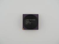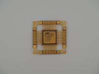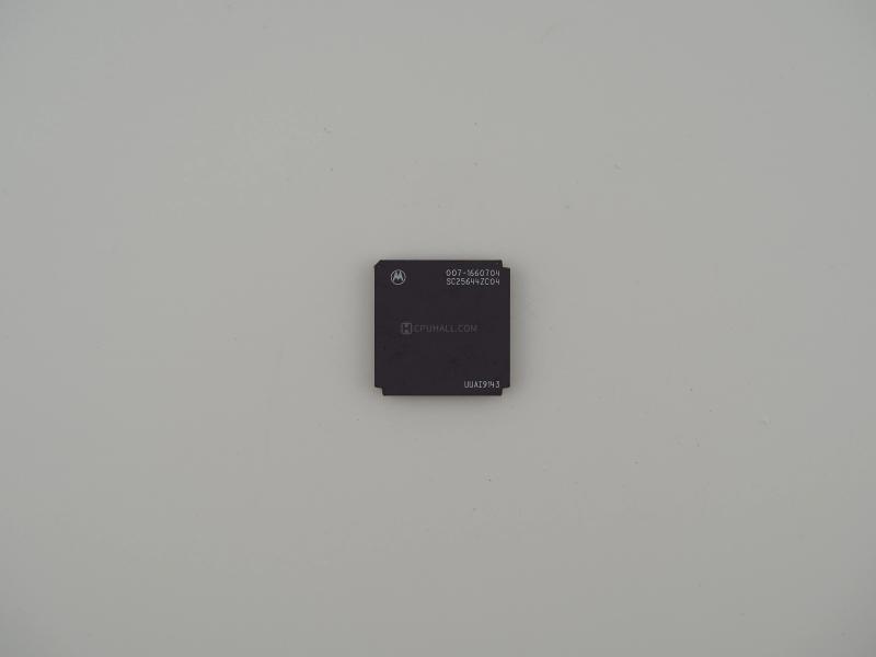
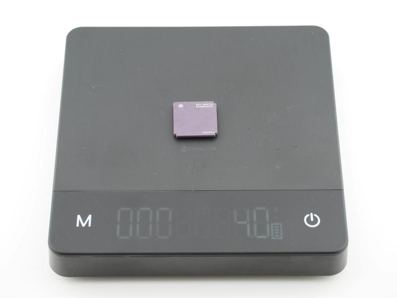
Placing it on the scale, it weighs in at exactly 4.0 grams. It is a dense, compact slab of early 1990s engineering. The top face features a beautifully austere, dark purple tinted ceramic substrate. The micro-contrast of the surface reveals a slightly porous, matte texture typical of high-grade aerospace or industrial ceramics from that era.
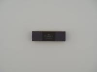
The laser etching on the top is crisp and perfectly legible:
(M)       007-1660704
          SC25644ZC04

          UUAI9143
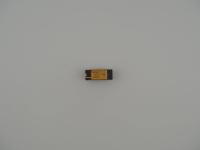
Flipping this artifact over reveals the true visual payload. The underside is a stunning 68-pin Ceramic Leadless Chip Carrier (CLCC) configuration. The gold plated traces radiate outward from a central, raised dark ceramic square like a sunburst. This central square is the hermetic seal protecting the silicon die within. The condition of the gold plating on these pads is exceptional, showing almost no oxidization or insertion wear, suggesting this specific unit might be New Old Stock (NOS) or a perfectly preserved spare. The aesthetic contrast between the deep black of the central seal, the rich yellow of the gold traces, and the purple-grey ceramic body is pure heavy metal hardware perfection.
Diving into the technical weeds, this package is a masterclass in robust design. The CLCC-68 form factor was highly favored in the late 1980s and early 1990s for environments where thermal stability and physical durability were paramount. Unlike plastic packages that can absorb moisture and crack during reflow soldering, this ceramic body is virtually impervious to environmental degradation.
The gold pads on the bottom are not just for visual flair. They provide an incredibly low resistance connection point for surface mounting, or for insertion into a specialized high-retention socket. The way the traces are routed out from the central cavity indicates a relatively straightforward lead frame, but the sheer size of the central cavity suggests a decently sized silicon die inside.
Given the 1991 date code, the fabrication node is likely somewhere in the 1.0 micron to 0.8 micron range. While we do not have a traditional clockspeed for a custom logic chip like this, chips in this package and era typically operated anywhere from 16 MHz to 33 MHz, depending on their role on the motherboard. The thermal dissipation of this package is excellent, meaning whatever this silicon was doing, it likely ran warm enough to justify the expense of ceramic over plastic, but not so hot that it required a massive external heat spreader.
This chip belongs to the shadow world of custom silicon. Motorola was an absolute juggernaut in the late 80s and early 90s, not just for their legendary 68000 series microprocessors, but for their custom application specific integrated circuit (ASIC) division. The "SC" prefix in the part number stands for "Special Component" or "Semi-Custom".
These were chips designed to order. A major client would come to Motorola with a specific logic requirement, perhaps needing to consolidate an entire board of discrete TTL logic chips into a single, reliable package to save space and power. Motorola would mask the logic onto their silicon and package it up. Because these were proprietary to the customer, there are no public datasheets, no marketing materials, and no grand press releases.
There is a fun hardware myth that every "SC" Motorola chip is a secret military component. While Motorola certainly built silicon for defense contractors, the reality is usually more grounded. These custom ASICs powered everything from high-end UNIX workstations and telecom routing gear to arcade cabinets and industrial automation controllers. They are the unsung heroes of vintage computing.
As a collector, pieces like this are an absolute joy to investigate because they require forensic deduction. Let us walk through the evidence.
The manufacturer is undeniably Motorola, confirmed by the classic stylized "M" logo enclosed in a circle. We know it is a custom or semi-custom ASIC due to the SC25644ZC04 marking. The ZC suffix often indicates the specific package type in Motorola's internal nomenclature, aligning perfectly with the ceramic surface-mount format we observe.
The date code UUAI9143 is our Rosetta Stone for the timeline. It tells us this chip was manufactured in the 43rd week of 1991. The UUAI prefix likely denotes the specific Motorola fabrication plant and the wafer batch.
The true mystery lies in the top number: 007-1660704. This is almost certainly the client's internal inventory or part number. Companies like Apple, Sun Microsystems, Silicon Graphics, and Hewlett-Packard notoriously stamped their own part numbers on custom silicon. While Apple part numbers often follow a 344S- format, and SGI frequently used 030- or 070- for boards, the 007- prefix is highly specific. Without a confirmed schematic from the original host machine, identifying the exact function of this logic block remains an educated guess.
Based on the era, the expensive ceramic packaging, and the part number format, my strongest hypothesis is that this artifact belongs to high-end telecommunications infrastructure equipment or a specialized industrial control system from the early 90s. It remains a beautiful, cryptic puzzle piece in the museum, representing the bespoke engineering that once dominated the tech industry.