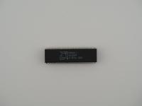
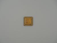
At first glance, this is a completely standard 40-pin Dual In-line Package. It weighs precisely 6.0 grams and measures out exactly as a vintage DIP-40 should. But when I you look over the top casing, the story got weird.
Here is the exact transcription of the top markings:
R6502AP
11450-12
MEXICO
1349 B50323-8
Right next to this text is the classic Rockwell International logo, looking like a stylized peace sign or a bird in flight. But look closely at the text itself. The laser etching is incredibly sharp. It has the distinct micro-contrast and clean burn marks of a modern, high-precision industrial laser.
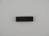
When I flipped the chip over to examine the underbelly, I found a completely different set of data molded directly into the plastic:
TAIWAN
L8404
We have a massive temporal anomaly here. The bottom plastic was molded in Taiwan with a date code of 1984 (8404). Yet the top surface claims it was assembled in Mexico with a laser-etched date code pointing to the 49th week of 2013 (1349). The pins are standard tin-plated copper, showing mild oxidation but remaining perfectly straight.
To understand this artifact, we have to talk about the silicon inside. The 6502 architecture is an absolute masterpiece of minimalist engineering. Originally designed by Chuck Peddle and his team at MOS Technology, the layout uses roughly 3,510 transistors. By stripping out complex instruction sets and focusing on an incredibly efficient pipeline, they created a chip that was vastly cheaper and often faster than the competition from Intel or Motorola at the time.
The "A" in the R6502AP designation indicates this specific die is rated for 2 MHz operation. While 2 MHz sounds laughable today, this processor accomplished a tremendous amount of work per clock cycle. The thermal constraints on this chip are practically non-existent by modern standards. It runs perfectly cool in this standard plastic package without any need for active heat dissipation or even a heat sink. The complexity here is not in the packaging, which is as basic as it gets, but in the enduring perfection of the underlying logic.
The historical prestige of the 6502 cannot be overstated. This is the architecture that built the personal computing revolution. It powered the Apple I and II, the Commodore VIC-20 and 64, and the Nintendo Entertainment System. It was the beating heart of the Atari 2600.
A common myth is that the 6502 died out in the late 1980s when the IBM PC standard took over the world. That is entirely false. While it left the desktop computer market, the 6502 architecture found a permanent home in embedded systems. It was used in everything from automotive engine control units and industrial pacemakers to military hardware and medical devices. The core design was so reliable and so well understood that engineers simply refused to stop using it.
When you see a chip with a 1984 package mold and a 2013 laser etch, the immediate instinct is to call it a counterfeit. The vintage hardware market is flooded with fake chips where unscrupulous sellers sand down generic microcontrollers and laser-etch famous part numbers onto them. However, I am highly confident this is not a malicious remark.
Instead, this artifact is a fascinating piece of sanctioned silicon history. Companies like Rochester Electronics or Lansdale Semiconductor specialize in buying up the original mask rights, intellectual property, and leftover raw die banks when a company like Rockwell officially exits a specific semiconductor business. They do this to support military, medical, and heavy industrial clients who have legacy systems built around the 6502 architecture that absolutely cannot be redesigned or upgraded.
It is entirely possible that an authorized legacy manufacturer took over production to fill a commercial order. They could have easily utilized a tray of New Old Stock blank plastic packages that were molded in Taiwan back in 1984. Fast forward to late 2013, an industrial client desperately needs a batch of replacement R6502APs. The authorized fab wire bonds the genuine, stored Rockwell dies into those 1984 vintage Taiwan blanks, then uses a modern, high-precision laser to etch the exact original Rockwell branding, the required fab designation, and the current 2013 date code (1349) along with their internal batch trace code (B50323-8).
This practice is incredibly common in the legacy silicon market. It perfectly explains why the laser etching looks far too clean and modern for a 1980s chip, why the date code is from 2013, and why the physical plastic package was molded in 1984. It is a completely genuine, authorized continuation chip assembled decades after the silicon was first conceptualized.