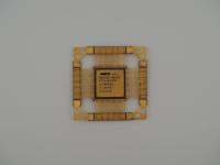
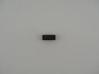
Holding this artifact under the macro lens, I am immediately drawn to the stunning contrast between the dark ceramic package and the heavy gold plating. This is a 68-pin LCC (Leadless Chip Carrier), and it is a textbook example of high-end industrial manufacturing. Weighing exactly 4.6 grams, it feels dense and substantial for its compact roughly 24mm square footprint.
The top surface features a matte black ceramic lid, laser-etched with the following markings:
TEK US
155 0289 02
420 087
Flipping this piece over reveals a fascinating story. The bottom is a stark, flat slab of dark purple-tinted ceramic. Unlike standard processors, there are no pins or center pads here. Instead, the gold contacts are strictly castellations wrapped around the outer edges. The absolute center of the bottom substrate is covered in a highly textured, silvery residue. This heavy scuffing and oxidation strongly suggest this chip was intimately bonded to a dense thermal pad or a custom heat spreader during its operational life.
Tektronix did not build these custom ICs for general computing. They built them to push the absolute physical limits of signal acquisition. In the era when this chip was fabricated, off-the-shelf silicon simply could not handle the extreme bandwidths, rapid sweep rates, or precise trigger timings required by high-end oscilloscopes.
The LCC-68 package chosen here was a deliberate engineering necessity. Leadless Chip Carriers provide incredibly short electrical paths from the silicon die to the PCB socket, which minimizes parasitic inductance and capacitance. When you are dealing with high-frequency analog signals or high-speed digital timing logic, every millimeter of pin length degrades the signal. Furthermore, the thick ceramic substrate acts as a critical thermal mass. These custom bipolar and early CMOS ASICs ran exceptionally hot, requiring the ceramic body to rapidly wick heat away from the fragile die inside to maintain stable performance characteristics.
In the vintage hardware and test equipment repair communities, the Tektronix 155- series of chips commands a massive amount of respect and a fair bit of dread. Tektronix operated their own specialized semiconductor fabrication plant in Beaverton, Oregon. They were essentially a silicon foundry operating entirely to serve their own instrument division.
Because these chips were entirely proprietary, they are the ultimate "unobtainium" today. If a custom ASIC like this dies in a vintage 2400-series or 11000-series oscilloscope, you cannot simply buy a modern replacement. You have to harvest a donor chip from another broken unit. This has created a cult following around these specific ceramic squares. They are the beating hearts of some of the greatest analog and early digital test equipment ever manufactured.
When researching this specific unit, the visual clues leave absolutely no room for doubt regarding its origin. The TEK US stamp and the 155- prefix perfectly align with the internal numbering scheme used by Tektronix for their monolithic integrated circuits.
While I can authoritatively identify the manufacturer and the package type, pinning down the exact function of the 155-0289-02 requires navigating a labyrinth of vintage service manuals. Tektronix produced hundreds of variations of these custom chips for tasks ranging from channel switching to display sequencing. The 420 087 marking likely acts as a batch identifier or a specialized date code indicating a manufacturing run. Regardless of its exact role in the circuit block, this piece is a beautiful surviving fragment of an era when hardware companies had to literally invent and bake their own silicon to achieve their engineering goals.