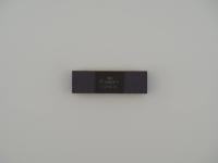
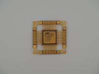
Weighing in at exactly 11.3 grams, this artifact feels incredibly substantial. It is a weaponized slab of white ceramic. Looking closely at the top cap, we see the unmistakable logo of the VZPP plant out of Voronezh, a stylized arrow emerging from the center of a tilted square. Below that logo, the Cyrillic text is sharply printed onto the metal lid.
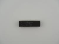
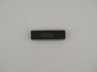
Part Number: KM1818 BM01A (Cyrillic: КМ1818ВМ01А)
Date Code: 9010 (10th Week of 1990)
Manufacturer Logo: VZPP (Voronezh Semiconductor Devices Factory)
Back Stamp: 353
Notice the solitary gold trace routing from the brazed cap down to a corner pin. This is a grounding strap designed to shield the die from electromagnetic interference, a feature you absolutely love to see on vintage hardware. Turning it over, the unglazed white ceramic substrate features a faint, unevenly inked 353 stamped onto the back. The 50 side-brazed gold pins are pristine and reflect the light brilliantly. It is a gorgeous piece of engineering.
Let us talk about the engineering because this chip is a brilliant freak of nature. Underneath that gold lid lies a direct Soviet clone of the Signetics 8X300. The 8X300 was originally designed by Scientific Micro Systems around 1975. It is a bipolar Schottky processor. Bipolar TTL logic meant it ran incredibly hot and drew a massive amount of power compared to MOS chips, but the tradeoff was raw, unadulterated speed.
The clock requirements were satisfied by an 8 MHz crystal, giving this chip a blistering 250 nanosecond instruction cycle time. It possessed a highly unusual architecture. The data bus was 8-bit, but the instructions were 16-bit wide. It featured dedicated hardware units for shift, rotate, mask, and merge operations. It could pull data from memory, manipulate it at the bit level, and push it back out to an I/O port all in a single clock cycle. It was effectively one of the very first digital signal processors ever made.
The history of this architecture is pure Cold War espionage and industrial necessity. Signetics produced the American version of this chip for high speed disk controllers, avionics, and specialized military communications. The Soviets needed that exact same capability for their own radar systems and missile guidance computers. Instead of inventing a completely new architecture from scratch, they simply reverse engineered the American design.
The irony here is that by the time the VZPP plant was stamping these out in 1990, the 8X300 architecture was already considered ancient by Western engineering standards. Yet, the Soviets packaged it in this utterly gorgeous, no expense spared CDIP-50 form factor. Fifty pins is an incredibly weird footprint for a dual inline package. It is practically a hallmark of the 8X300, and seeing it executed with Soviet military grade gold and ceramic is a wildly satisfying collision of worlds.
Identifying this piece for the collection was an absolute joy. The 50-pin layout is the immediate smoking gun. Very few integrated circuits in history ever adopted a DIP-50 package. When I combine those 50 pins with the Soviet Cyrillic markings and 1818 series code, it is definitively a clone of the Signetics 8X300. The logo explicitly ties it to the Elektronika Voronezh Semiconductor Devices Factory.
The "KM" prefix officially denotes a commercial or industrial grade ceramic package, but do not let that designation fool you. The materials used here are strictly high end. The heavy gold plating, the pristine ceramic substrate, and the thick metal cap are standard traits of the Soviet aerospace industry. The 9010 date code places the manufacturing of this clone squarely in March of 1990, right at the twilight of the Soviet era. It is a perfect time capsule.