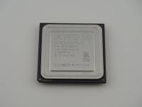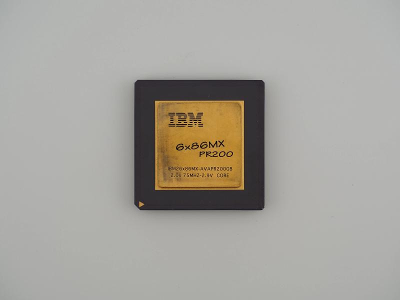
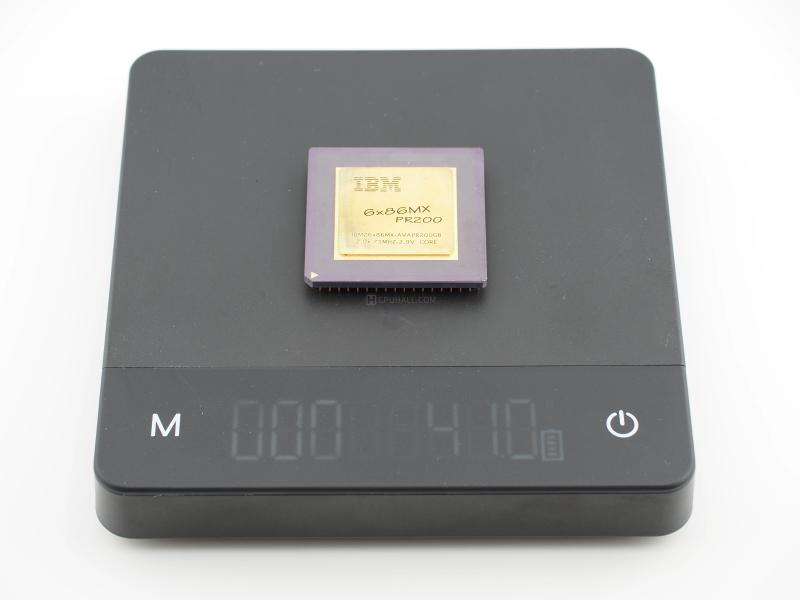
Dropping it on the digital scale, it clocks in at exactly 41.0 grams of late-nineties silicon and ceramic. It feels dense and substantial. The deep, almost aubergine purple of the ceramic substrate provides a gorgeous contrast to the massive gold-plated heat spreader sitting right in the center.
The surface markings are etched cleanly into the gold cap, revealing everything we need to know:
Front Cap:
IBM
6x86MX
PR200
IBM26x86MX-AVAPR200GB
2.0x 75MHZ-2.9V CORE
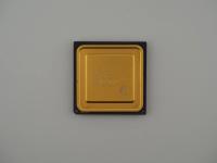
Back Die (Visible between pins):
COPR. CYRIX
1995,96,97 USA
IBM9314 R44090
01L4889 PQ
Flipping the chip over reveals a perfectly straight bed of gold pins and the central silicon die exposed on the bottom. I absolutely love looking closely at the back of this board. You can clearly read the Cyrix copyright text printed directly on the silicon packaging. The chamfered corner with the gold triangle marker on the top left of the ceramic base is pristine, showing no signs of brutal socket insertions. This artifact has survived the decades beautifully.
This is where the numbers get fun. Despite the "PR200" prominently stamped on the gold cap, this chip absolutely does not run at 200 MHz. The laser etching clearly states its actual math: a 2.0x multiplier running on a somewhat unusual 75 MHz front-side bus. That results in a true internal clock speed of exactly 150 MHz.
Cyrix engineered the 6x86MX (originally codenamed the M2) to go head-to-head with the Intel Pentium MMX. They bumped up the internal L1 cache to a massive 64KB, which was double what Intel was offering at the time. However, getting this chip to run stable was a known headache for system builders. The 2.9V CORE marking is critical. Earlier Socket 7 motherboards delivered a flat 3.3V to the processor. Dropping this chip into an older single-plane motherboard without voltage regulation would immediately fry it. You needed a newer dual-plane board that could feed 2.9V to the core and 3.3V to the I/O ring.
Furthermore, very few motherboards natively supported a 75 MHz bus in 1997. Most standard boards maxed out at 66 MHz. If you ran this chip at 66 MHz with a 2.0x multiplier, it clocked in at 133 MHz and severely bottlenecked the performance, destroying the "PR200" illusion entirely.
This processor represents one of the most brilliant and chaotic periods in the x86 clone wars. Cyrix was a fabless semiconductor company. They had brilliant engineers but no actual factories to bake their silicon. To get their chips made, they struck deals with foundries like SGS-Thomson and, notably, IBM. The deal was simple: IBM would manufacture the chips for Cyrix, and in return, IBM got to keep a large percentage of the wafers to brand and sell themselves. That is why I have a chip sitting here with a massive IBM logo on the front and a Cyrix copyright stamped on the back.
The Performance Rating (PR) system is the true legacy of this chip. Cyrix knew their architecture was far more efficient per clock cycle at integer math than Intel's Pentium. They argued that their 150 MHz chip performed just as fast as an Intel Pentium running at 200 MHz in standard Windows desktop applications. So, they slapped "PR200" on the box. Intel hated it, consumers were constantly confused by it, and AMD eventually adopted it for their own Athlon line years later.
There is a dark side to the Cyrix legacy. While the integer performance was incredible for Microsoft Word or Excel, the floating-point unit (FPU) was objectively terrible. If you built a rig with this exact chip in 1997 and tried to boot up Quake, you were going to have a bad time. Intel processors decimated Cyrix in 3D gaming because John Carmack's engine relied heavily on raw FPU calculations. This chip earned an unfair reputation as "garbage" solely because it could not run Quake smoothly, despite being an absolute beast for everyday computing.
I do not need to guess with this piece. The physical evidence is conclusive and paints a perfect picture of the 1997 foundry agreement between Cyrix and International Business Machines.
The exact part number IBM26x86MX-AVAPR200GB decodes perfectly against historical data books.
Seeing the 1995,96,97 copyright on the back firmly places this unit right at the launch window of the MMX-compatible M2 core generation. It is a textbook example of late-nineties alternative silicon. It is an artifact from a brief window in time when a buyer could walk into a computer store and realistically choose between Intel, AMD, Cyrix, IDT, or even an IBM-branded desktop CPU for their home PC.