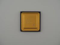
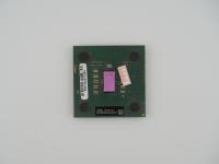
Placing it on the scale reveals a solid weight of 36.3 grams. Holding this artifact, I am immediately struck by the aggressive, permanently bonded black heatsink dominating the top surface. It feels like a piece of military hardware rather than a consumer PC component.
Here is the exact transcription of the laser-etched text on the front face:
intel®
OVERDRIVE™
DX2ODPR66
C4430640
SZ904 V3.0
[M][C] 1989 1992
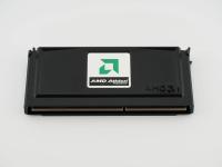
Flipping the chip over reveals a completely different aesthetic. Embedded in the dark ceramic substrate is a brilliant, highly reflective gold cap covering the silicon die. The gold-plated pins are perfectly brazed in a classic grid layout with an empty inner square and one keyed corner for socket orientation. The micro-contrast captures some light dust nestled between the heavy heatsink fins, a testament to its age and the environment it once operated in.
The rear gold cap bears its own distinct factory markings:
94284176CA
A4
FJ 43
The raw technical leap this piece of silicon represents is incredible. The DX2ODPR66 is a masterclass in extending the lifespan of existing platforms. Operating at 5 volts, this chip utilized clock-doubling technology. The host motherboard would feed the processor a 33 MHz external bus clock, and an internal phase-locked loop multiplier would drive the internal core up to a blazing 66 MHz.
Underneath that gold cap lies a piece of silicon packing roughly 1.2 million transistors manufactured on Intel's 0.8-micron process. Squeezing that much logic into this footprint and running it twice as fast as the system bus generated a serious thermal load. That is exactly why Intel engineered this chip with the integrated black anodized heatsink. Standard 486 chips often ran bare or with cheap aftermarket fans, but the OverDrive required guaranteed thermal dissipation straight out of the retail box. It also features 8KB of integrated L1 cache to ensure the faster internal core was not constantly starved for data by the slower external bus.
Intel completely rewired the consumer mindset regarding PC upgrades with the OverDrive series. Before these chips hit the market, a CPU upgrade often meant ripping out the entire motherboard or engaging in risky crystal oscillator swaps that could destabilize the entire system.
The "OverDrive" marketing campaign was pure genius. It sounded fast, aggressive, and incredibly easy. You just pulled out your old, slow 33 MHz chip and dropped this heavy metal block into the socket. Instantly, your spreadsheet calculations and Doom framerates doubled. There is a common myth that all OverDrive chips required a special secondary socket on the motherboard. While some motherboards did feature a dedicated OverDrive socket for the ODP variants, this specific ODPR (OverDrive Processor Replacement) was designed to aggressively evict and replace the original CPU entirely.
Visual evidence strongly confirms the identity and purpose of this specific artifact. The SZ904 S-Spec is the golden key here. It definitively identifies this as the 5V retail replacement part designed for a 33 MHz system bus.
The dual copyright years of 1989 1992 tell a clear historical story. The 1989 date covers the original underlying 80486 architecture patents, while 1992 marks the introduction of the DX2 clock-doubling IP. The text V3.0 indicates a later stepping of the voltage regulator or internal silicon revision. The rear gold cap markings 94284176CA and FJ 43 represent internal fabrication lot numbers and assembly facility codes. The presence of the gold cap on the bottom rather than the top is a fascinating packaging choice necessitated by the top-mounted heatsink design, forcing the die cavity to the underside of the ceramic substrate. It is a brilliant, dense, and historically pivotal piece of computing history.