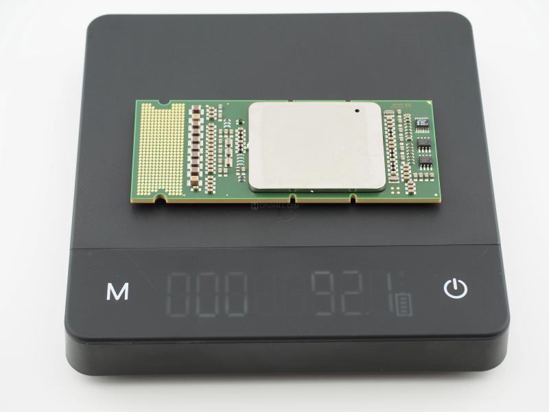
Placing this artifact on the scale, it registers at an incredibly satisfying 92.1 grams. This is not a fragile piece of consumer electronics; it is an unapologetic block of enterprise hardware.
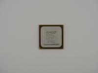
Using macro lighting to pull the faint laser etchings from the surface, I can clearly transcribe the identification data off the rear substrate:
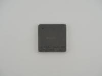
Front IHS:INTEL(R) ITANIUM(R) 2
i (M) (C) '06 (e4)
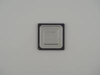
Rear Substrate:9020 1.42/12M/533/400
SL9PB COSTA RICA
3648B179-0068
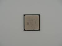
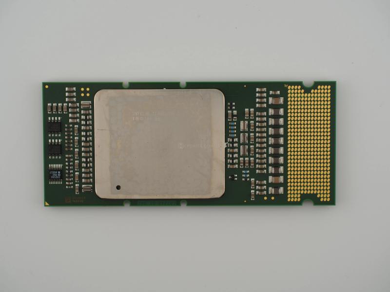
The physical layout of this processor is striking. Built on a rectangular green PCB, the massive polished silver Integrated Heat Spreader (IHS) dominates the center. Flanking the silicon are two distinct zones. On the right wing, a neat arrangement of exposed surface mount capacitors and logic chips are visible, including clearly marked Atmel 24C01A I2C serial EEPROMs and 1021AA logic ICs. On the left wing, there is a dense, perfectly aligned grid of gold pads. The entire package feels rugged, brutalist, and over-engineered.
Diving into the silicon underneath that heavy IHS, we are looking at the "Montecito" core. Released in 2006, the Itanium 2 9000 series was a massive engineering undertaking. Manufactured on Intel's 90nm process node, this specific unit packs a staggering 1.72 billion transistors. To put that into perspective, the vast majority of that transistor budget was dedicated to the massive 12MB on-die L3 cache.
The 9020 designation points to a dual-core processor clocked at 1.42 GHz with a 533 MHz Front Side Bus. The power delivery required for a chip of this magnitude was intense. The PAC611 (Pin Array Cartridge) form factor essentially turns the CPU into a miniature self-contained motherboard. The Atmel EEPROMs visible on the surface likely functioned as a Processor Information ROM (PIROM), feeding crucial voltage and thermal parameters to the server motherboard before the system even fully powered on. The thermal challenges of dissipating heat from nearly two billion transistors in 2006 dictated the use of that massive, thick IHS and the heavy-duty mounting hardware standard to Socket 611 platforms.
The Itanium architecture has a dark, fascinating history. Often jokingly referred to as the "Itanic" by hardware enthusiasts, IA-64 was Intel and HP's massive gamble. The idea was to completely replace the aging x86 architecture with Explicitly Parallel Instruction Computing (EPIC). They believed the future of computing relied on the compiler doing the heavy lifting of instruction scheduling, rather than complex out-of-order execution hardware on the chip itself.
It was an incredibly ambitious failure. The x86 emulation layer on early Itanium chips was painfully slow, and compilers struggled to efficiently optimize code for the EPIC architecture. Meanwhile, AMD executed a brilliant flanking maneuver by releasing the AMD64 extension, allowing standard 32-bit x86 software to run natively alongside 64-bit code. The industry flocked to AMD64, forcing Intel to adopt the same standard for their consumer and mainstream server lines.
Despite losing the broader market war, Itanium chips like this Montecito unit found a dedicated home in mission-critical, high-uptime environments running HP-UX. This processor represents the absolute peak of that stubborn, heavy-metal era of bespoke server design.
Based on the pristine SL9PB S-Spec laser etching on the rear substrate, identifying this artifact as an Intel Itanium 2 9020 is straightforward and definitive. The date code 3648 indicates this specific unit was manufactured in the 48th week of 2006 at the Costa Rica fabrication plant.
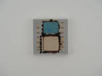
However, the high-fidelity macro shots reveal some fascinating physical quirks. While traditional PAC611 packages often featured delicate, protruding pins on the bottom, the rear of this PCB is entirely flat. Furthermore, studying the extreme close-ups of the gold contacts reveals massive, thick gold bars and heavy-duty decoupling capacitors. These thick gold bars are completely distinct from traditional signaling pads. This suggests that this specific module may have interfaced with a high-density Land Grid Array socketing mechanism or a proprietary high-amperage power delivery slot inside a specific OEM blade server chassis. It is a brilliant example of how enterprise hardware often required custom physical interfaces simply to feed enough clean power to the silicon.