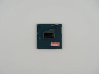
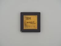
When I dropped this specific unit onto the scale, it weighed in at exactly 19.5 grams. The top side is clean and minimal, featuring six surface-mount capacitors flanking the central slug. The laser etching on the metal is faint but undeniable, revealing the classic intel pentium logo, a 2D data matrix, and i166.
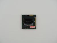
Flipping it over to the pin side reveals where the real forensic work begins. Nestled deep within the gold Staggered Pin Grid Array (SPGA) is a raised black epoxy block containing the actual silicon. I put it under the macro lens to pull the white markings directly off the potting compound:
intel pentium
FV80502166
SY037/VSU
ICOMP® 2 #=127
A4
C6501173-0517
(m)(c) '92'93
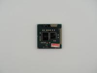
The pins are completely straight, and the gold plating still retains a brilliant, heavy metal luster. The surface texture of the dark fiberglass substrate feels incredibly dense, a perfect snapshot of mid-90s hardware engineering.
Diving into the technical weeds, this chip represents a fascinating transition period for portable computing. The 80502 designation marks this as a P54C core. Pushing 166 MHz in a tightly packed laptop chassis in 1996 presented a massive thermal challenge. Intel solved this bottleneck by utilizing Voltage Reduction Technology (VRT).
By splitting the internal voltage rails, the core could run at a battery-sipping 2.9V while the external I/O remained at the standard 3.3V to interface with typical motherboard chipsets. This was a critical architectural quirk that kept laptops from melting straight through desks. The VSU code present on the epoxy specifically confirms this split-voltage capability.
The mid-90s mobile processor market was an absolute Wild West of packaging standards. Before the rigid, predictable days of the Mobile Module Connector (MMC-1 and MMC-2), manufacturers were desperately trying to figure out how to cram desktop x86 power into plastic clamshells.
This era birthed incredible rivalries and some truly bizarre hardware configurations. The prevailing myth at the time was that mobile Pentiums were just aggressively downclocked desktop chips. In reality, the integration of VRT and the specialized thermal packaging meant these were heavily binned and highly specialized pieces of silicon. The 166 MHz model was the absolute speed limit for this specific mobile line before the Tillamook MMX cores rendered them obsolete.
This is exactly where this specific piece becomes a brilliant forensic mystery. The part number FV80502166 explicitly designates a Tape Carrier Package (TCP). A naked TCP chip has no pins at all; it is just a piece of polyimide film with microscopic gold traces designed to be directly soldered to a laptop motherboard.
Yet, I am holding a chip with a Pin Grid Array.
So, what exactly is sitting in my collection? My extensive research into vintage Intel databooks points to one clear conclusion. This is a factory TCP silicon package that has been professionally mounted onto an organic PGA interposer. These adapters were utilized for a few specific reasons. Sometimes they were used internally in labs to test TCP yields in standard Socket 7 ZIF testbeds. Other times, third-party upgrade companies bought bulk TCPs and mounted them on these PCBs to sell as laptop upgrades for machines that utilized socketed CPUs rather than soldered boards. The black potting compound on the underside is the dead giveaway, it protects the fragile TCP tape bonds right where they mate with the dark interposer board. It is a fantastic, physical bridge between two wildly different packaging eras.