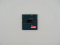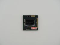
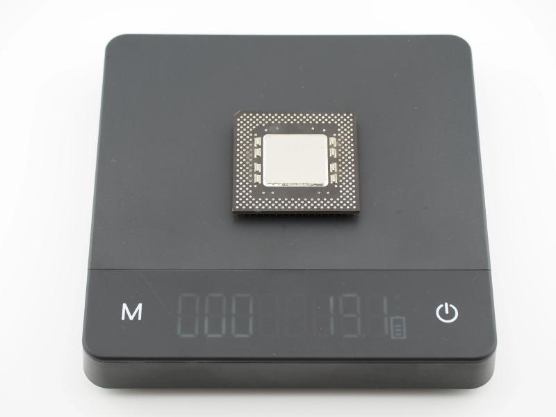
Holding this artifact in my hand brings a very specific heft and texture. Throwing it on the scale reveals a mass of exactly 19.1 grams. This specific unit represents a major transitional era in laptop computing packaging. When looking at the top face, we see a heavy metallic heat spreader designed to interface directly with a laptop cooling assembly. The surface features a faint, micro-contrasted laser etching alongside a rudimentary 2D matrix barcode.
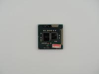
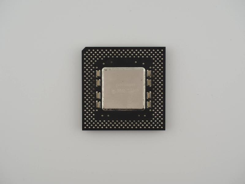
Flipping the processor over reveals the true engineering charm. Instead of a solid ceramic belly, we have a dense array of gold plated pins surrounding a deep central cavity. The substrate itself is a dark, rigid plastic. This is the Plastic Pin Grid Array packaging. The critical identification data is stamped deep inside this recessed cavity.
Top Face Etching:[2D Matrix Barcode]
intel
pentium
w/ MMX™ tech
Bottom Cavity Markings:intel®
pentium®
w/ MMX™ tech
FV80503233
SL27S / 2.5V
MALAY
L9490269-0319
m(c) '92 '95
The contrast between the bright gold pins, the dark brown organic substrate, and the silver heat slug gives this piece a strictly utilitarian, heavy metal vibe. You can see a few surface-mounted capacitors flanking the top heat spreader. These are placed as close to the silicon as possible to decouple the power supply and keep the voltage clean.
Underneath that metal cap lies the Intel P55C core. This was a massive architectural leap disguised as a minor revision. Intel took the original Pentium architecture and grafted on 57 new instructions specifically designed to handle vector processing. This was Single Instruction Multiple Data processing brought to the consumer x86 market.
To accommodate these new multimedia execution units, the transistor count jumped from 3.3 million in the classic Pentium to 4.5 million. The L1 cache was also doubled to 32KB to feed the hungry new SIMD pipelines. All of this was fabricated on a 0.35 micrometer CMOS process.
Because this is a mobile part, power delivery was a massive hurdle. Desktop MMX chips typically ran at a 2.8V core voltage. This mobile variant was engineered to run at a significantly lower 2.5V core voltage. This dual voltage requirement meant the motherboard had to supply 3.3V to the external I/O pins to talk to the rest of the system while stepping down the voltage specifically for the core logic. This PPGA form factor allowed OEMs to plug a desktop class processor right into the cramped chassis of a late 90s thick laptop without instantly melting the battery.
You cannot talk about the P55C without talking about the marketing blitz. Intel poured hundreds of millions of dollars into making "MMX" a household name. They put their engineers in brightly colored bunny suits and danced them across television screens worldwide. Consumers had no idea what a SIMD instruction was, but they absolutely knew they needed MMX Technology to make their games run faster.
The myth at the time was that an MMX chip would automatically make everything look better. The reality was that software had to be explicitly written to take advantage of the new registers. If you ran a standard integer based program on this chip, it was essentially just a classic Pentium with a slightly larger cache. However, when paired with optimized software like early software video decoders or 2D rasterizers, the performance leap was staggering. This specific mobile chip powered the legendary "desktop replacement" laptops of the era. These were absolute bricks of machinery that could finally play CD-ROM games on the go.
There is no mystery regarding the identity of this artifact. The physical markings provide absolute confirmation. The S-Spec number SL27S is the definitive identifier in Intel's taxonomy. Consulting the Intel processor specification updates confirms that SL27S corresponds directly to a 233 MHz Mobile Pentium MMX.
Furthermore, the part number FV80503233 breaks down perfectly. The FV prefix denotes the Plastic Pin Grid Array mobile package. The 80503 string is Intel's internal designation for the P54/P55 family architecture. The 233 suffix dictates the clock frequency. The L9490269 batch code tells us this specific silicon was rolled out of the Malaysia fabrication plant around the 49th week of 1999, which makes it a very late production run for a chip architecture introduced in early 1997. It is a brilliant, heavy piece of mobile computing history.