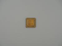
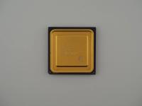
Holding this piece, the first thing I notice is the satisfying density of the dark ceramic package. It weighs exactly 8.8 grams on the scale and measures roughly 3.5 centimeters square. This specific unit is a pristine example of late-eighties silicon packaging. The micro-contrast highlights the crisp, laser-etched markings on the top face.
The surface text reads exactly as follows:
(M)
MC68030RP33B
09D66C
CNEIG0835

MCIGCN  JAPAN
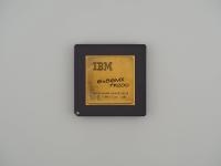
Flipping the artifact over reveals a classic staggered gold-plated pin array. The brazing on the pins is immaculate. What really stands out on the underside is the central cavity. Instead of an exposed die or a gold-plated lid, this specific unit features a flush, dark green epoxy or polymer fill protecting the silicon. It creates a striking visual contrast against the dark ceramic and the brilliant gold pins.
This chip represents a massive leap forward in integrated engineering for its era. The Motorola 68030 was essentially the ultimate refinement of the legendary m68k architecture before the radical superscalar redesign of the 68040. Packed with approximately 273,000 transistors and fabricated on a 0.8-micron process, this was heavy metal compute power for the late 1980s.
The primary engineering triumph of the 68030 was integration. Motorola took the core of the preceding 68020 and brought the Memory Management Unit directly onto the die. Previously, systems required an expensive and hot external 68851 MMU to handle virtual memory. Integrating it reduced latency and motherboard complexity.
Furthermore, this architecture implemented a modified Harvard architecture internally. It featured dual independent 256-byte caches for instructions and data. While 256 bytes sounds comical today, having on-die memory operating at full core speed allowed the processor to fetch instructions and data simultaneously without fighting over the external bus. Running at 33 MHz, this specific processor would have been a top-tier performer, requiring a decent heatsink to dissipate the thermal load generated by that dense cluster of active transistors.
The 68030 is royalty. If you did any serious creative work, programming, or high-end desktop publishing in the late 1980s to early 1990s, you were likely sitting in front of a machine powered by this exact architecture.
It was the beating heart of the Macintosh IIci, the Amiga 3000, and a whole slew of formidable UNIX workstations from Sun Microsystems and HP. Perhaps most famously, a 68030 powered the original NeXT Computer. The legendary black cube that Tim Berners-Lee used to invent the World Wide Web was driven by this very silicon family.
A common myth among retro hardware enthusiasts is that the 68030 was just a die-shrunk 68020. That is entirely false. While the instruction execution unit was largely identical, the integration of the MMU, the addition of the data cache, and the completely redesigned internal bus structure made it a vastly more efficient beast clock-for-clock. It was the absolute standard-bearer for CISC processors before the RISC revolution of the mid-1990s began to aggressively challenge Motorola's dominance.
The provenance of this artifact is highly clear thanks to the impeccable legibility of the surface markings. The MC68030RP33B part number authoritatively identifies it as a 33 MHz part in a ceramic Pin Grid Array package.
The string 09D66C is the silicon mask revision. Motorola frequently updated their masks to fix microcode bugs or improve yield. The 09D66C mask is a known, late-revision stepping that is highly stable.
The MCIGCN JAPAN text at the bottom indicates the fabrication origin. During this era, Motorola partnered heavily with Japanese foundries like Tohoku Semiconductor to keep up with the massive global demand for m68k processors. The 0835 date code in the third line is fascinating. While the architecture launched in 1987, Motorola continued manufacturing the 68030 for decades for industrial and embedded applications. Given the specific font and the green polymer backing, I suspect this particular unit was manufactured much later than the original 1980s run, likely serving in high-reliability networking gear or specialized industrial control hardware before making its way to my archive.