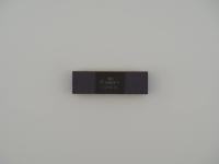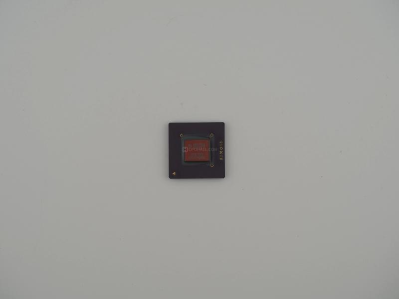
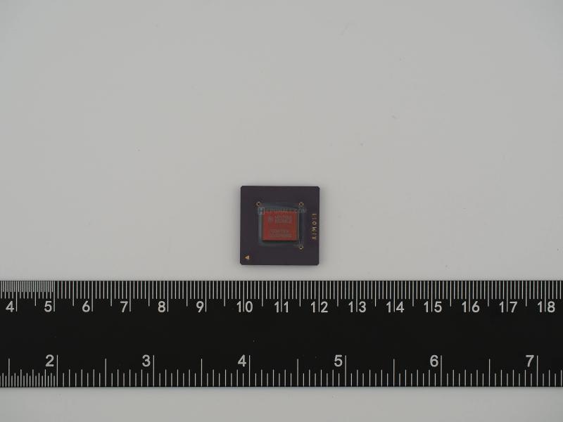
Placing this specific unit on the scale, it registers a mere 3.0 grams. It is a remarkably compact piece of silicon engineering. Measuring roughly 21mm by 21mm, this processor is dominated by the exposed, copper-tinted rectangular die sitting perfectly center on a dark organic substrate.
Holding this piece under macro lighting, the manufacturing details are striking. The die is secured with a translucent, gray underfill epoxy that pools slightly around the edges. The laser-etched text on the top of the die is faint but highly legible, featuring the iconic stylized Motorola "M" logo.
Here is the exact transcription of the surface markings:
(M) MPC740A
RX266LH
00K19S
QCJ0408C
Substrate marking (right edge):A1M011
Flipping the chip over reveals a flawless Ball Grid Array. The 256 solder balls are arranged in a strict grid, untouched and completely pristine. The overall aesthetic has a very industrial, no-nonsense vibe that perfectly represents late 1990s embedded hardware.
To understand what we are looking at here, we have to look at the legendary PowerPC G3 architecture. This chip contains the exact same "Arthur" core as the famous PowerPC 750, but with one critical architectural amputation. Motorola deliberately removed the backside L2 cache interface.
By stripping away the interface required to talk to external high-speed cache SRAM, Motorola engineers were able to drastically reduce the pin count. The PowerPC 750 required a massive 360-pin package to handle the extra data bus. This MPC740A, however, fits comfortably into a much smaller 256-ball BGA package. This made it cheaper to produce, easier to integrate into tight PCB layouts, and highly power efficient.
The A suffix in the model name indicates a die shrink. While the original 740 was fabricated on a 0.29-micron process, the 740A was shrunk down to 0.25-micron technology. This allowed it to hit its 266 MHz clockspeed with lower thermals, making it an absolute powerhouse for environments that could not afford active cooling.
The PowerPC alliance was formed by Apple, IBM, and Motorola to crush Intel. When people think of the G3 generation today, their minds immediately go to the candy-colored iMacs that saved Apple from bankruptcy. The PowerPC 750 was the golden child that graced the covers of tech magazines.
The MPC740 was the unsung, blue-collar worker of the PowerPC family. Because it lacked the L2 cache bus, it was not suited for high-end desktop computing. Instead, Motorola aggressively targeted the embedded market. This architecture was shoved into enterprise network routers, telecom switches, and specialized industrial controllers. It did the heavy lifting in the background of the early internet infrastructure.
There is a fun misconception that all PowerPC chips of this era ran incredibly hot. While the high-end workstation chips definitely required serious heat dissipation, chips like this 740A were praised precisely for their thermal efficiency. The bare-die design we see here allowed for excellent direct-to-heatsink thermal transfer in cramped embedded enclosures.
The laser etchings leave no room for ambiguity. The MPC740A clearly identifies the core and revision. In Motorola's part numbering scheme for this era, the RX prefix before the speed grade explicitly denotes the Ball Grid Array package type, which matches the physical evidence on the bottom of the chip perfectly.
Furthermore, the 266 confirms the operating frequency of 266 MHz. The date code QCJ0408C is particularly interesting. The 0408 strongly suggests this specific unit was manufactured in the 8th week of 2004. This proves that while the architecture launched in 1997, it had an incredibly long production lifecycle, serving the embedded market for well over half a decade after its introduction.