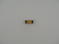
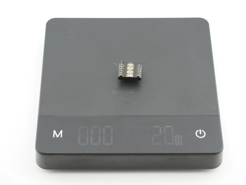
When observing this artifact resting on the digital scale, it weighs a mere 2.0 grams. Against the ruler, the entire package measures barely 17 millimeters across. It is essentially a tiny technological insect frozen in amber.
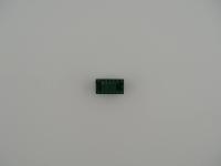
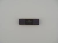
When looking at the back of this board under magnification, the dark substrate reveals an incredibly intricate network of embedded gold routing traces leading to the 12 exterior pins. Right in the center of the underside, there is a very distinct logo that tells a fascinating manufacturing story.
Visible Surface Markings:Logo: Stylized "N" (National Semiconductor)
Back Substrate: Embedded gold routing traces
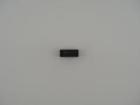
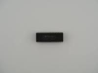
Pinout: 12 pins (6 per side, 0.1 inch spacing)
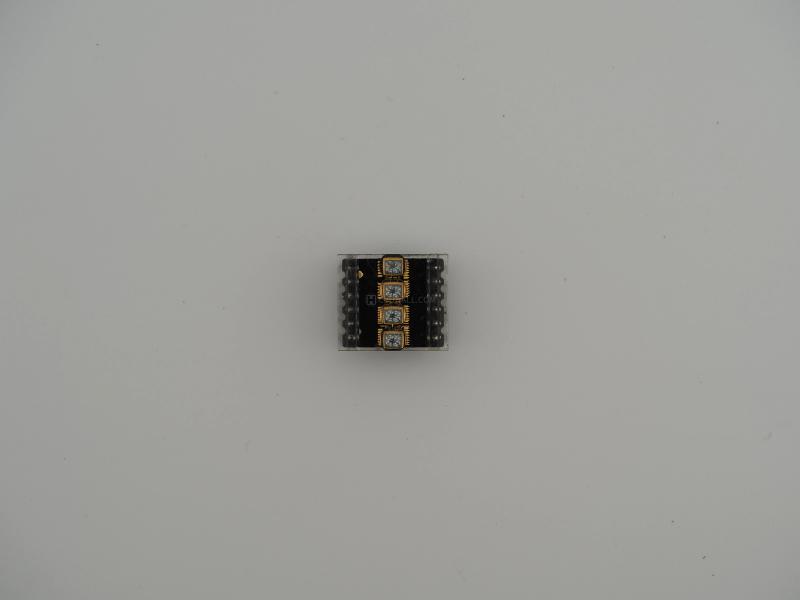
Die Layout: 4 individual 16-segment alphanumeric dies
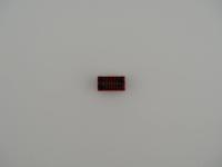
Flipping it over to examine the top, the artifact truly shines. We have four individual Gallium Arsenide Phosphide (GaAsP) monolithic dies mounted perfectly in a row. Over each die sits a cast clear epoxy dome. Looking deep into those magnifying domes reveals the undeniable "Union Jack" diagonal starburst pattern of a 16-segment alphanumeric display. The pristine condition of the pins tells me this specific unit was likely never socketed or soldered. It is a flawless example of late 1970s smart optoelectronics.
Let us dive into the technical weeds of how this little marvel actually operates. The engineering difference between a basic 7-segment calculator display and this DL1414 highlights a massive evolutionary leap in embedded systems.
A standard LED bubble display is a "dumb" component. It is nothing more than raw diodes wire-bonded to a fiberglass substrate. To make a standard display show a character, the host microprocessor must physically drive current through the specific anode and cathode pins, multiplexing at high speed across all the digits to trick the human eye into seeing a solid shape. This takes up massive amounts of CPU overhead.
The DL1414 is an "Intelligent Display". It actually contains a monolithic CMOS integrated circuit buried inside that dark plastic package right alongside the LEDs. That onboard silicon includes a RAM memory bank, an ASCII character generator, and all the multiplexing LED drive circuitry. A microprocessor simply sends a standard 7-bit ASCII data code and a 2-bit address to the DL1414 pins. The embedded chip handles all the heavy lifting of figuring out which microscopic gold wires to energize to illuminate the correct starburst segments. It keeps those segments lit from its own internal memory without requiring the host CPU to constantly refresh it.
By the late 1970s and early 1980s, engineers building complex industrial gear, test equipment, and early synthesizers needed a way to display error codes and alphanumeric text. They could not afford to burden their early, slow processors with tedious LED refreshing loops. The DL1414 stepped in to solve that exact problem.
This component is legendary in the vintage computing world. You will frequently find them clustered in long rows on the front panels of extremely expensive 1980s logic analyzers, Hewlett-Packard lab equipment, and legendary drum machines. The 12-pin layout was explicitly designed without vertical overhangs so engineers could stack them perfectly end-to-end to create continuous scrolling text marquees.
There is a fascinating bit of corporate cross-pollination here as well. The DL1414 was originally designed and popularized by Litronix, which was later acquired by Siemens. However, the demand for these smart alphanumeric displays was so astronomical during the golden age of embedded hardware that other semiconductor giants stepped in to fabricate them. Seeing the classic National Semiconductor logo stamped on the back of a classic Litronix/Siemens footprint is a wonderful testament to the second-sourcing practices of the era.
The visual evidence on this piece is absolute and decisively confirms its identity.
The initial tell is the pin count and geometry. The 12-pin footprint features exactly six pins spaced 0.1 inches apart on each side. This perfectly matches the DL1414 specification for end-stackable modularity. Standard "dumb" calculator displays almost universally utilized 14-pin layouts to handle the raw multiplexing matrix lines.
The absolute smoking gun is found under the epoxy lenses. A macro examination of the die structure reveals the complex 16-segment layout required to draw the English alphabet, complete with the diagonal traces needed for letters like "K", "R", and "X". Standard numeric displays only possess a figure-8 structure. The combination of the 12-pin layout, the smart alphanumeric dies, and the National Semiconductor manufacturing stamp makes this a beautifully documented piece of hardware history. It perfectly bridges the gap between the raw diodes of early calculators and the dot-matrix LCD screens that would eventually conquer the world.