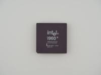
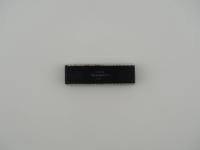
Placing it on the scale, it weighs in at exactly 4.8 grams. This specific unit features a gorgeous dark purplish-brown ceramic substrate, a material choice that feels undeniably premium compared to the flexible organic packages that took over the industry shortly after.
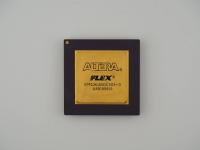
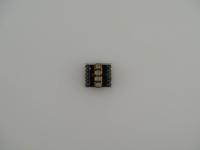
Under the macro lens, the exposed flip-chip die is a brilliant, reflective blue. It is framed by a perimeter of white underfill epoxy to protect the delicate microscopic solder bumps connecting the silicon to the ceramic. Flanking the die are six prominent surface-mounted decoupling capacitors, three on each side, designed to smooth out the power delivery for that 1.25 GHz core.
The laser etching on the fragile bare die is perfectly preserved. Here is the exact transcription of the surface text:
(Motorola Batwing Logo) MOTOROLA
SICOH
1.25 GHZ
EVT Q27
SAMPLE
04L64M
QZZ0313Z
(Substrate Bottom Center): 7440
(Substrate Right Edge Vertical): S24001W001 B (with an upward triangle)
(Substrate Bottom Left): 1
Flipping this artifact over reveals a flawless 19x19 ball grid array. Doing the math, a full 19x19 grid equals 361 contacts. Observing the top right corner, exactly one ball is omitted for orientation indexing. That leaves us with exactly 360 pins, securely identifying the package as a standard CBGA-360.
Diving into the silicon itself, a 1.25 GHz clockspeed on a Motorola chip from this era tells a very specific story. We are looking at the twilight of the PowerPC G4 architecture. Early G4 chips, like the original MPC7400, generated massive amounts of heat and struggled to scale past 500 MHz. To hit 1.25 GHz without melting the surrounding motherboard, Motorola had to shrink the manufacturing process down to a 0.13-micron Silicon-on-Insulator (SOI) node.
The 7440 marking on the bottom of the ceramic is a massive clue to its engineering lineage. The Motorola PowerPC 744x series was intentionally designed for space-constrained environments like the Apple PowerBook G4 and high-end embedded network switches. Unlike the massive 483-pin MPC745x chips that included a dedicated L3 cache interface for desktop towers, the 360-pin package of this chip drops the L3 cache support entirely. This allowed Motorola to shrink the footprint dramatically, relying entirely on the fast, on-die 512KB L2 cache.
Because this is an Engineering Verification Test (EVT) sample, this silicon represents the very messy, iterative process of hardware development. The engineers in Austin, Texas were likely pushing this specific stepping (Q27) to its absolute thermal limits to validate the 1.25 GHz target before mass production.
The history surrounding this era of Motorola silicon is legendary. In the early 2000s, Apple was trapped in a fierce marketing war with Intel. Intel was aggressively pushing the Pentium 4 to ridiculous, blazing-hot clockspeeds. Meanwhile, Motorola was hitting a brick wall trying to scale the PowerPC G4.
This led Apple to invent the famous "Megahertz Myth" marketing campaign. They argued that a 1.25 GHz G4, armed with its massive AltiVec SIMD vector processing unit (which Apple branded the "Velocity Engine"), could absolutely obliterate a 2.0 GHz Pentium 4 in clock-for-clock efficiency. And for workloads like Photoshop or video encoding, they were absolutely right.
This specific sample was minted in early 2003, right on the precipice of a massive corporate shift. By 2004, Motorola would spin off its entire semiconductor product sector into a new company called Freescale. Therefore, this chip is one of the final heavy metal artifacts to bear the iconic Motorola batwing logo before the branding vanished from desktop computing forever.
While the physical characteristics perfectly align with an early MPC7447 prototype, the SICOH laser etching on the die makes this one of the weirdest artifacts in my entire collection.
Usually, an EVT sample from this family will explicitly say "XPC7447" on the die. The word SICOH is completely undocumented in standard Motorola databooks. Initially, I suspected it might be a stylized etching of RICOH. Ricoh heavily utilized PowerPC architecture for their massive, enterprise-grade Aficio multifunction printers. However, looking closely at the macro photography, the first letter lacks the vertical left stem of an 'R'. It is unequivocally an 'S'.
My working theory is that SICOH was either an internal Motorola codename for a specific fab run, or a custom ASIC project for a client that utilized the PowerPC e600 core.
Furthermore, the 7440 printed on the ceramic substrate does not mean the chip itself is an MPC7440. The original MPC7440 never officially reached 1.25 GHz. Instead, it was standard practice for Motorola to reuse the exact same 360-pin CBGA substrate from the older 7440 line to test new 7447 silicon. Why tool a brand new ceramic package for an EVT sample when the pinout is identical?
The date code 0313Z hidden in the lot number translates to the 13th week of 2003. This perfectly aligns with the development timeline of the MPC7447, which Apple eventually deployed in their final generation of Aluminum PowerBook G4s later that year. It is a stunning, mysterious piece of transition-era silicon.