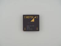
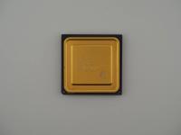
Clocking in at 47.6 grams on the scale, this artifact feels like a proper weapon. The package is a 4.5cm square of dark, almost purplish-brown ceramic, which contrasts violently with the massive, gleaming gold heat caps.
Taking a close look at the top surface, the laser etching is crisp and authoritative.
NEC JAPAN
D30700RS-180
VR10000
9647E9006 ES2.6
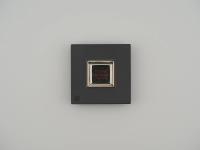
Flipping the chip over reveals the true beauty of this packaging. Instead of fragile pins, the bottom features a beautifully arrayed Ceramic Land Grid Array (CLGA). The gold contact pads perimeter a massive central gold thermal slug. The tactile feel of the ceramic edge is perfectly smooth, and the gold plating on the central die caps shows only minor surface variations under macro light. It is a flawless example of mid-90s premium engineering.
The silicon beneath that gold cap is an absolute monster for its era. The MIPS R10000, code-named "T5" during development, was a 64-bit advanced superscalar microprocessor. This specific unit operates at 180 MHz, which required some serious electrical and thermal engineering to keep stable.
The architecture features out-of-order execution, which was a massive leap forward for the MIPS instruction set. To achieve this, the die packed roughly 6.8 million transistors, usually fabricated on a 0.35-micron process. Pushing that many transistors at 180 MHz in 1996 generated an immense amount of heat. That explains the massive gold plates on both the top and bottom of the CLGA package. The central bottom slug wasn't just for show. It was designed to interface directly with thermal dissipation solutions in the socket, ensuring the die did not literally cook itself under heavy workstation loads.
If you watched a blockbuster movie in the late 1990s, there is a very high probability that the CGI was rendered on a machine powered by this architecture. The MIPS R10000 was the beating heart of Silicon Graphics (SGI) workstations like the legendary Octane, the Indigo2, and the massive Origin 2000 servers.
While SGI and MIPS designed the architecture, they did not have their own foundries. They relied heavily on partners like NEC and Toshiba to actually bake the silicon. That is why this chip carries the fierce NEC VR10000 branding. At the time, this chip was locked in a brutal, high-stakes war against the DEC Alpha 21164 and the Intel Pentium Pro. The R10000 was infamous for its floating-point performance, making it the undisputed king of 3D geometry calculations.
The markings on this chip tell a very clear and exciting story. The ES2.6 designation proves this is an Engineering Sample, specifically revision 2.6 of the silicon. This means it was used for internal testing, motherboard validation, or sent out to close partners before the final retail chips hit the market.
The date code 9647 is highly revealing. It indicates the chip was packaged in the 47th week of 1996, placing its birth right at the end of November. The D30700RS-180 part number directly corresponds to NEC's internal cataloging for the VR10000 family, with the -180 suffix confirming the 180 MHz clock speed. Finding an engineering sample of a workstation-class chip from this era is a rare treat, and it earns a permanent, highly visible spot in the archive.