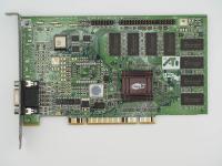
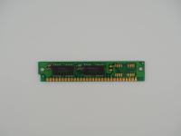
Holding this piece, I immediately noticed the quintessential late 1990s ASUS aesthetic. The amber, almost golden PCB is a massive nostalgia trip that instantly dates the hardware. This specific unit weighs in at exactly 105.7 grams and represents the absolute basement of 3D acceleration for its era.
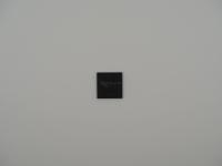
Looking closely at the central silicon, the BGA package is completely exposed, lacking any active cooling fan or even a passive aluminum heatsink. This naked presentation was a defining trait of extreme budget cards from this period. The surface text on the main chip is crisply laser-etched and reveals the classic early NVIDIA stylized logo:
NVIDIA (Stylized Logo)
RIVA TNT2 TM 64
VANTA (Printed Vertically)
T3B5C15530015
S1 TAIWAN
Flanking the GPU are four Hyundai SDRAM chips. The micro-contrast under the photography lights reveals their exact batch and model identifiers:
HYUNDAI KOREA
HY57V161610D
TC-7
0025A
The board itself proudly proclaims TNT2-VANTA REV 1.00 directly above the GPU and carries the classic ASUS brand mark on the right side. On the bracket, we have a single, unassuming 15-pin VGA connector molded in a vibrant blue plastic.
Underneath that dark BGA substrate lies the NV5 architecture. This was NVIDIA's 250nm powerhouse design, but the Vanta was strictly bred for the budget bin. While the full-fat TNT2 enjoyed a robust 128-bit memory bus, this Vanta is choked down to a highly restrictive 64-bit interface.
The core chugs along at a modest 100 MHz. The four HY57V161610D Hyundai memory chips are 16-megabit SDRAM ICs, meaning this board is equipped with exactly 8MB of local video memory. The TC-7 suffix on the RAM indicates a 7-nanosecond access time, rating the chips for up to 143 MHz, though NVIDIA typically clocked Vanta memory around 110 MHz or 125 MHz to maintain strict product segmentation.
The complete absence of a heatsink proves just how little thermal output this heavily cut-down chip produced. It runs incredibly cool, drawing minimal power strictly through the AGP slot without needing any supplemental external power connectors.
The late 90s graphics market was an absolute bloodbath. NVIDIA was fighting 3dfx for the performance crown, but the real financial war was won in the pre-built OEM market. The Vanta was NVIDIA's ultimate trojan horse.
By stripping down the phenomenal TNT2 architecture, cutting the memory bus in half, and lowering the clock speeds, they created a dirt-cheap silicon package. Companies like HP, Compaq, and Dell could slap these into every family computer sold at big box retail stores.
The Vanta is absolutely not glamorous. Hardcore gamers and 3dfx Voodoo loyalists laughed at it. If you tried to play Quake III Arena on this card at high resolutions, you were watching a slideshow. But from a historical perspective, this exact tier of silicon is why NVIDIA captured massive, undeniable market share. It generated the massive revenue streams that eventually gave them the capital to buy out the bankrupt remains of 3dfx just a few years later.
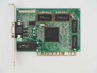
Tracing the exact origins of this artifact required looking past the bold ASUS branding on the front. When flipping the board over, a distinct set of white barcodes breaks up the golden trace lines:
5184-3926 1.00-A05
071016-C1AVH0-A05-00528
06CT152600
I instantly recognized the top number format. The string 5184-3926 is a classic Hewlett-Packard spare part number format. Running this through my archival databooks confirms that this specific card was originally shipped inside an HP Pavilion desktop PC. ASUS manufactured the board as a direct OEM contractor for Hewlett-Packard.
Furthermore, looking back at the memory chips, the 0025A date code on the Hyundai RAM indicates the memory was packaged in the 25th week of the year 2000. This perfectly aligns with the turn-of-the-millennium timeline when HP was refreshing their consumer desktop lines with budget AGP graphics to support Windows 98 SE and the upcoming Windows ME environments.