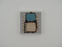
Holding this piece in my hand, the first thing that strikes me is the incredible contrast of materials. We have a classic mid-1990s green fiberglass laminate substrate topped with a brilliant, highly reflective gold-plated heat spreader. It is a stunning little artifact that perfectly captures the transitional era of packaging technology.
Under the macro lens, the laser etching on that gold cap is incredibly crisp. The classic overlapping "U" Sun Microsystems logo sits proudly in the top left, followed by the stylized "Sun" typeface. Here is the exact transcription of the surface text:
Sun
BGA 25©1994,SMI
PSTP1080BGA-83
F645012AGFP
H9504926
5AN4JKJ 980
JAPAN
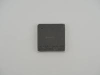
Dropping this onto the scale, it registers at a featherweight 5.4 grams. Placing it against the ruler reveals exactly why the first line of text reads "BGA 25". The chip measures precisely 25mm by 25mm. Flipping it over, we see a perimeter Ball Grid Array (BGA) layout featuring four rows of solder balls wrapping around a dark, central epoxy resin zone that protects the underside of the silicon die. The pristine condition of the gold cap and the intact solder balls suggest this piece might be New Old Stock (NOS) or was very carefully extracted.
This artifact represents a fascinating period in silicon engineering. By 1994, the industry was desperately trying to move away from massive, pin-heavy ceramic packages (like the PGA) for chips that did not strictly require them. Laminate BGA packaging allowed for denser board designs, better electrical characteristics for high-speed signals, and lower manufacturing costs.
However, heat was still a problem. The solution here is that beautiful gold square. It serves as an integrated heat spreader (IHS). Instead of slapping a heavy copper lid over the entire package, Sun and their manufacturing partners bonded this gold-plated metal plate directly over the die area on top of the laminate. Gold is exceptionally resistant to oxidation and provides excellent thermal conductivity, making it the perfect material to interface with whatever heatsink or thermal pad was mounted above it in the tight confines of a 1U server or a pizza-box workstation.
The JAPAN origin and the F645012AGFP part number strongly point to Fujitsu as the silicon foundry. During the 1990s, Fujitsu was Sun's right-hand manufacturing partner, fabricating everything from massive SuperSPARC processors to the intricate glue logic that held Sun's proprietary motherboard architectures together.
Back in the 1990s, Sun Microsystems was an absolute juggernaut in the enterprise and workstation markets. They did not just build computers; they engineered entire ecosystems. While companies like Intel were pushing generic beige boxes, Sun was designing custom UNIX workstations with proprietary buses (like the SBus and MBus) and highly specialized memory controllers.
The lore of Sun hardware from this era is filled with custom ASICs (Application-Specific Integrated Circuits). A SPARCstation motherboard was a sea of these square green and gold chips, each handling a very specific task. You had chips dedicated to memory arbitration, chips translating SBus signals to Ethernet, and chips managing the massive crossbar switches required for multi-processor communication. These auxiliary chips are the unsung heroes of the UNIX boom. They never got the marketing glory of the main SPARC processors, but without them, the servers would be absolutely useless bricks of silicon.
Identifying the exact function of this specific artifact requires some serious detective work because the "PSTP1080BGA-83" part number does not correspond to a mainline SPARC processor.
Here is my thought process as I break down the evidence. We know Sun used the "STP" prefix for many of their custom chips. For context, the MicroSPARC I was the STP1010, and the MicroSPARC II was the STP1012. Seeing "STP1080" immediately makes me wonder if this is an obscure, highly integrated embedded SPARC core. The "83" at the end of the first line could theoretically denote an 83 MHz clock speed, which falls right in line with the 70 MHz to 110 MHz range of mid-90s MicroSPARC parts.
However, looking at the second string, F645012AGFP, we find a massive clue. That is a classic Fujitsu gate array format. Fujitsu's F60000 series were standard CMOS gate arrays used to build custom logic controllers. The fact that this is a gate array strongly points away from it being a central processor.
Therefore, I am highly confident that this piece is a specialized ASIC used in a Sun SPARCstation or early Ultra Enterprise server. Given the 1994 copyright and the mid-1995 date code (9504 indicating the 4th week of 1995), this chip was likely pushing data across an SBus interface, managing SCSI traffic, or acting as a memory buffer in a machine running Solaris 2.4. It remains a slight mystery precisely which data path it controlled, but it stands as a brilliant physical testament to Sun's absolute dominance of custom 90s server silicon.