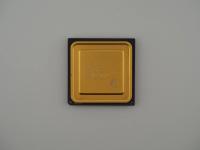
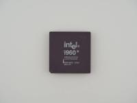
Dropping this onto the scale, it registered exactly 32.2 grams. We are looking at a masterclass in early 2000s hardware aesthetics. The substrate is a gorgeous, deep plum-purple ceramic, offering a stark and beautiful contrast to the massive gold-plated heat spreader dominating the top.
The surface text on the gold cap is laser-etched with incredible clarity. The warnings and specifications can be transcribed:
VIA
C3 Processor
TM
VIA C3 -800AMHz
(133 x 6.0)
HEATSINK/FAN REQUIRED
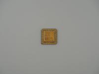
Flipping the chip over to examine the pin array reveals pristine, gold-plated Socket 370 pins. They are perfectly straight, showing no signs of brutal socket insertions. Dead center on the bottom of the ceramic, nestled right within the pin field, is a dark, smooth epoxy-filled region carrying the factory fabrication marks:
(C)(M) VIA C3 TM
1.65V AG40XT0
0249 TAIWAN
308851-04
The micro-contrast on these lower etchings is faint but legible. The tactile feel of the ceramic edges is sharp and industrial. It is a fantastic artifact that feels more like a piece of jewelry than a budget desktop processor.
To understand what is happening inside this purple and gold tile, we have to look past the VIA branding. This is the handiwork of Centaur Technology, specifically the C5B "Samuel 2" core architecture.
While Intel was ramping up the hyper-pipelined NetBurst architecture for the Pentium 4 and AMD was pushing the aggressive Athlon Thunderbird, Centaur took a completely different path. The Samuel 2 core was manufactured on a 150nm (0.15-micron) fabrication node. It featured an incredibly short 12-stage integer pipeline. This made the processor vastly more efficient per clock cycle for basic operations but severely limited its maximum clock speed scaling.
This specific 800 MHz unit utilizes a 133 MHz Front Side Bus (FSB) with a 6.0x multiplier. The bottom text explicitly states a core voltage of 1.65V. The gold heatspreader on top was a necessary addition to protect the fragile silicon die underneath from the crushing force of heavy Socket 370 cooler mounting clips, a common issue that routinely cracked exposed Pentium III dies.
One of the great architectural quirks of the Samuel 2 core was its cache arrangement. It packed a massive 128KB L1 cache (split evenly between instructions and data) but only a paltry 64KB L2 cache. This strange ratio actually ran exclusively, meaning data was not duplicated between the L1 and L2 caches, maximizing the available on-die SRAM.
The history of the VIA C3 is a story of sheer survival. VIA Technologies wanted their own x86 license, so they went on a shopping spree and bought both Cyrix and Centaur Technology. While Cyrix had the name recognition, their core designs were struggling. VIA wisely chose to ditch the Cyrix technology and put all their money behind Glenn Henry and his Centaur engineering team in Austin, Texas.
The C3 became legendary not for its speed, but for what it lacked. The Floating Point Unit (FPU) in the Samuel 2 architecture ran at half the speed of the core clock. If you tried to play a 3D game like Quake III Arena on this processor, it would absolutely crawl compared to an identically clocked Intel Celeron. The gaming community mercilessly mocked it.
However, the joke was ultimately on the critics. Because the C3 was so incredibly power-efficient, it became the undisputed king of the emerging embedded, industrial, and thin-client markets. The text on the gold cap screaming HEATSINK/FAN REQUIRED is actually a fantastic piece of hardware irony. These chips ran so incredibly cool that system builders routinely ripped the fans off and ran them completely passively in completely silent mini-ITX media centers. It was the ultimate quiet rebel of the early 2000s.
Identifying the exact silicon beneath that gold cap requires piecing together the surface clues. I can state with absolute authority that this is a Centaur C5B "Samuel 2" core, and not the later "Ezra" core.
The smoking gun is the core voltage printed on the underside: 1.65V. The subsequent Ezra cores transitioned to a newer 130nm TSMC process and dropped their voltage requirements down to 1.35V. The 1.65V requirement firmly anchors this chip in the 150nm Samuel 2 era.
Furthermore, the date code 0249 is fascinating. It indicates this processor was manufactured in the 49th week of 2002. By late 2002, the Samuel 2 architecture was already being phased out for newer designs, making this a very late-production run of this specific core variant. The TAIWAN marking confirms TSMC as the foundry, perfectly aligning with VIA's fabless manufacturing strategy. This artifact is a perfectly preserved slice of alternative x86 history.