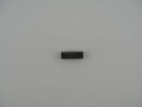
Looking at this specific artifact in my collection, the very first thing that commands attention is the gorgeous, deep purple ceramic substrate. This material choice is an absolute hallmark of high-end and aerospace-grade vintage silicon from the 1980s. Mounted on the front of this 30-pin Single In-line Package (SIP) are four individual dark epoxy chips, flanked by two tiny surface-mount decoupling capacitors neatly labeled "4" on the board.
The laser etching on the face of the four identical chips reads:
F 8266A-12
8447 G48
JAPAN
Flipping the module over, the back of the bare purple ceramic is sharply printed with white text:
F JAPAN MB85108A-12 8530 G15
The micro-contrast of the white text against the purple ceramic is incredibly crisp. The 30 straight through-hole pins along the bottom edge show standard solder tinning. They lack the thick gold plating we sometimes see on true military-spec hardware, but they remain remarkably straight and free of serious oxidation. The 8447 date code on the chips indicates the underlying silicon was fabricated in the 47th week of 1984, while the substrate was assembled slightly later in the 30th week of 1985 based on the 8530 stamp.
To understand what we are looking at, we have to dive into the technical realities of 1980s memory fabrication. This artifact is a 256K-bit memory module. Because building a monolithic 256K die was incredibly difficult and plagued with terrible yields at the time, engineers simply mounted four smaller 64K-bit (65,536 x 1-bit) MB8266A Dynamic RAM chips in parallel onto one stick.
The MB8266A chips themselves were serious performers. Fujitsu fabricated these using a silicon-gate NMOS process with an advanced double-layer polysilicon design. This allowed for single-transistor memory storage cells, tightly packing over 65,000 transistors into each package. By strapping four of these together, this little ceramic stick holds roughly a quarter million transistors. The -12 suffix designates a 120ns row access time. This speed was highly optimized for heavy iron, specifically designed for mainframe memory buffers and high-speed peripheral storage. It also featured "CAS-before-RAS" refresh logic and a "Nibble Mode" allowing high-speed serial access to up to 4 bits of data at a time.
Holding this piece is like holding a physical relic of the brutal 1980s semiconductor trade wars. Modules exactly like this one are the precise reason American titans like Intel had to completely exit the DRAM market. Japanese manufacturers like Fujitsu perfected their manufacturing yields to such an extreme degree that they flooded the market with highly reliable, fast memory that domestic fabricators simply could not compete with.
There is a common misconception that all purple ceramic from this era was exclusively meant for military or aerospace contracts. While it is true that mil-spec components required ceramic packaging to prevent outgassing and thermal degradation, companies like Fujitsu frequently utilized these same stunning purple substrates for commercial high-end mainframe memory. Their fabrication lines were already highly optimized for it, and the aesthetic was a fantastic byproduct of their engineering standards.
Another fun quirk regarding SIP memory is the sheer anxiety it caused system builders. Before the industry completely shifted to SIMMs with flat edge contacts, these SIPs with their 30 delicate, breakable pins were the standard for dense memory expansion. You lived in constant fear of bending one of these fragile legs while forcing them into stiff, unforgiving motherboard sockets.
I am extremely confident in the identification of this artifact. The visual clues are unambiguous and line up perfectly with archival Fujitsu documentation. The MB85108A prefix explicitly designates the assembled SIP memory module itself, while the 8266A denotes the underlying 64K NMOS DRAM components. The timeline matches up flawlessly with the 1984 to 1985 transition period, right before 1 Megabit DRAMs became commercially viable and rendered these smaller parallel modules obsolete.