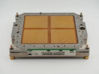
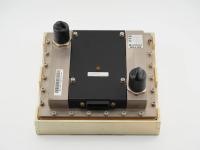
This is not your standard piece of late-century silicon packaging. What we are looking at is a magnificent, rectangular slab of cold, hard IBM heavy metal.
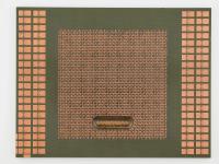
Looking closely at the top surface, the pristine white alumina ceramic is adorned with a perfectly symmetrical, dense grid of gold pads. These are C4 (Controlled Collapse Chip Connection) flip-chip sites, waiting for silicon die that were never mounted. The edges of the module are a stark, dark grey, revealing the microscopic horizontal striations of the internal routing layers.
Flipping it over, the bottom is a fortress of brazed gold pins, packed so tightly it looks like a high-end brush. The only visible marking on the entire artifact is a small, green stamp on the stepped white ceramic end block:
829
Given the revised identification of this piece, this date code likely translates to the 29th week of 1988, placing it squarely in the prime production era of the advanced IBM 3090 mainframes. The visual contrast between the stark white ceramic, the dark grey molybdenum edges, and the brilliant gold pins makes this one of the most aesthetically pleasing raw materials in my entire collection.
To understand what this artifact is, we have to dive into the absolute madness of IBM's packaging engineering. When IBM moved from the 308X series to the 3090 Mainframe, they pushed their Multi-Layer Ceramic (MLC) technology to its absolute physical limits. The 3090 relied on screaming-fast Emitter-Coupled Logic (ECL) chips that ran incredibly hot. To support the massive interconnect density required by these chips, the ceramic substrate had to be beefed up significantly.
The dark edges you see along the side of this stick are the visible cross-sections of up to 38 distinct layers of ceramic tape. IBM engineers would take raw alumina powder, mix it with a glass frit and an organic binder, and cast it into thin, flexible sheets. They would punch tens of thousands of microscopic vias into these sheets and screen-print the circuit traces using a conductive paste made of molybdenum.
These layers were then perfectly aligned, pressed together, and fired in a massive furnace at 1500°C. During the firing process, the entire substrate would shrink by roughly 17%. Controlling that shrinkage so that the top C4 pads and the bottom PGA pins still aligned perfectly was a metallurgical miracle. The increased thickness of this specific unit is the direct result of adding more power and ground planes to feed the hungry ECL logic of the 3090 architecture.
The East Fishkill facility where IBM manufactured these ceramics was less of a factory and more of a black-magic materials science laboratory. The full-sized substrates built using this process became the legendary Thermal Conduction Modules (TCMs). A single 3090 TCM could hold over 100 chips and required a complex, helium-filled, water-cooled hat just to keep it from melting down under the 500-plus watts of heat it generated.
There is a long-standing rumor in vintage hardware circles that a single raw, unpopulated TCM blank cost more to manufacture than a brand-new luxury car. Looking at the insane tolerances required to keep the molybdenum traces intact during the violent 1500°C shrinkage phase, I absolutely believe it. This era of IBM mainframe engineering represents a time when cost was irrelevant. If the laws of physics presented a barrier, IBM simply threw millions of dollars of materials science at the wall until the barrier broke.
Initially, pieces like this are easy to mistake for the earlier 3081 generation. However, putting this specific artifact side-by-side with a delidded 308X and a delidded 3090 TCM in the lab reveals the truth. The 308X substrate is noticeably thinner. This piece perfectly matches the massive, thickened layer stack of the 3090.
The most fascinating aspect of this artifact is its shape. Standard IBM TCM substrates from the 3090 mainframes are strictly square. This piece, however, is a long, narrow rectangle with specialized, stepped mounting tabs on the extreme ends.
So what exactly is it?
Examining the multi-layer edge profile and the exact layout of the C4 pads, there is zero doubt in my mind this is a specialized 3090-era MLC substrate. The "stick" form factor points to two distinct possibilities.
The first possibility is that this is an engineering test coupon or cross-section monitor. Monitoring the 17% shrinkage and ensuring the internal vias did not tear during the firing process was a daily nightmare for IBM engineers. It was common practice to co-fire test strips alongside the main production modules. These strips could be electrically probed or physically cross-sectioned to verify layer registration without destroying a priceless production blank.
The second, more intriguing possibility is that this is a specialized logic or cache slice designed for a peripheral controller board or a custom high-speed bus interface within the 3090 ecosystem. The stepped white ends look purposely designed to slide into a mechanical rail system, which you would not need for a simple test coupon. The dense, rectangular layout of the die sites suggests it was meant to hold a linear array of cache RAM or buffer logic.
Whatever its exact internal part number was, it stands today as a flawless, unpopulated canvas of the greatest era of heavy metal computing.