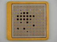
When I first held this heavy 176.2-gram slab of substrate, the sheer density and visual complexity immediately commanded respect. This artifact is a meticulously crafted demonstration cut-out sample of an IBM 3081 System Board.
Visible Identifiers and Markings:Grid X-Axis: A0 to F9 (60 columns)
Grid Y-Axis: 01 to 60 (60 rows)
Total Grid Area: 3,600 connection points
Total Weight: 176.2g
Feature: Milled trench exposing internal copper power planes
Look closely at that recessed oval in the center. That is not a functional cavity for a capacitor or an optical transceiver. It is an intentional milled trench created by IBM specifically to show off the internal structure of the board to executives and VIPs. You can literally see the thick, exposed copper power supply lines stepping down through the internal metal layers. The greenish patina on that exposed copper is just gorgeous, showing its age perfectly. The edge routing is clean because this piece was purpose-cut to be a display artifact, showcasing a tiny fraction of a monstrous 60x70cm multi-layer PCB.
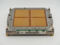
In 1980, connecting a processor to the outside world was a logistical and electrical nightmare. The IBM 3081 utilized the Thermal Conduction Module (TCM), an absolute brick of an engineering marvel containing up to 118 flip-chip logic dies. Each of those TCMs had exactly 1,800 pins on its underside. You could not just plug that into a standard motherboard.
IBM had to invent the most advanced printed circuit board in the world. The full-size 3081 System Board measured a staggering 60x70 centimeters, took six months to produce, and held up to nine of these 1,800-pin TCMs. To handle the dense signal routing and the colossal electrical current required by the Emitter-Coupled Logic (ECL) chips, the board was built with 20 metallic layers and 58 insulating layers. It contained roughly 1,000 meters of internal interconnects. The thick gold pads on the edges of this sample, and the densely packed 60x60 grid, give you a sense of the sheer I/O density. The current flowing through those milled copper planes would instantly vaporize a modern consumer motherboard.
Mainframe hardware from the IBM 3080 and 3090 era sits in a league of its own. There is a reason this era of IBM is often compared to the Apollo program of computing. They did not just design the chips. They designed the custom metallurgy, the ceramics, the extreme cooling arrays involving water chillers and helium-filled hats, and the colossal system boards required to hold them together.
The myth that modern multi-layer PCBs are somehow vastly superior to vintage tech gets completely shattered when you hold this piece. Even by today's automated standards, fabricating a massive board with 20 flawless layers of thick copper and high-speed signal routing is a manufacturing nightmare. Pieces like this milled display sample were literally handed around boardrooms to justify the multi-million dollar price tags of these machines. It was designed to make executives open their checkbooks by showing them exactly where their money was going.
The exact specifications of this heavily padded, multi-layered board lock this artifact in perfectly to the IBM System/370 Extended Architecture era.
The 1,800-pin count is the ultimate dead giveaway. That is the exact, heavily documented pin count of the 3081 TCM. The description of the 20 metal layers, the 58 insulated layers, and the massive currents all align flawlessly with IBM's published whitepapers on their early 1980s packaging technology. Furthermore, the 60x60 grid on this sample equals exactly 3,600 terminals, which aligns perfectly with IBM documentation detailing the massive 3,600-terminal cable connection blocks used on these system boards. What we have here is a rare survivor of IBM's internal promotional material. It is a physical infographic that puts modern hardware manufacturing to shame.