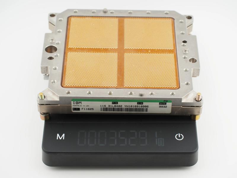
Holding this artifact requires two hands and a lot of respect. Putting this piece on the scale immediately validates its imposing presence. It weighs a staggering 3529.1 grams. That is over three and a half kilograms of precision-machined metal, dense glass-ceramic, and gold. It feels less like a piece of computing hardware and more like a critical component salvaged from a deep-space satellite.
IBM ASSEMBLED IN USA
P/N 11S 31L8402
S/N YH1016918986
PQ DATE 9932
E.C. F11625
Ceramic Substrate Etching: F918968
Weight: 3529.1 g
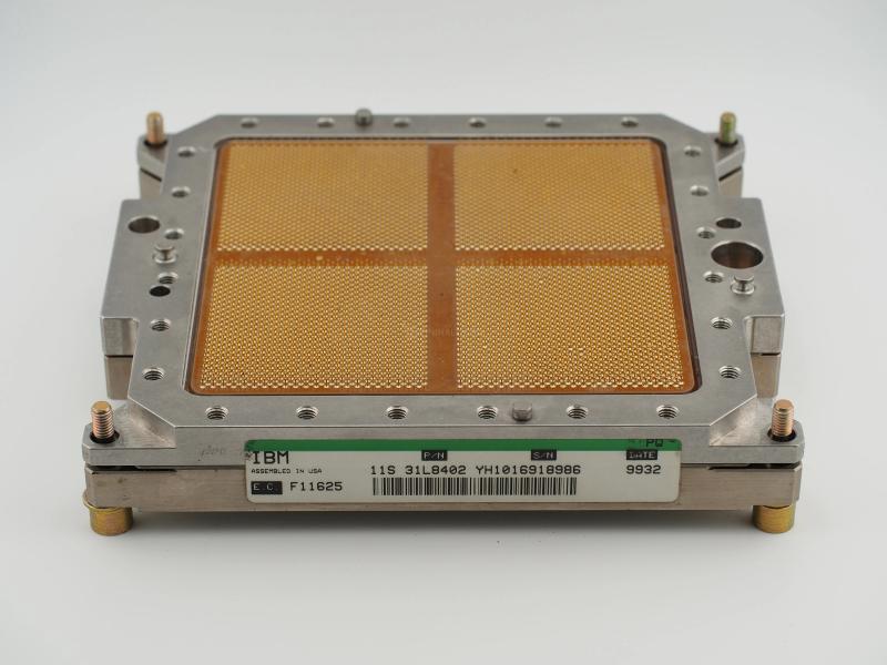
Looking at the top of the module, we see a heavy metal heat-spreader block secured by precisely torqued hex and torx fasteners. On the left side is a fascinating mechanical alignment bracket stamped with an "R" and what looks like a "1" or an "I" which would interface with the massive zero-insertion-force actuation mechanisms of a mainframe motherboard.
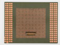
Flipping this colossal block over reveals an absolute sea of gold. The bottom consists of a thick, dark organic and glass-ceramic substrate divided into four highly dense quadrants of pins. Getting close to the substrate reveals the faint red-orange laser etching of the internal serial number F918968. The micro-contrast of the pins is breathtaking. Every single pin is perfectly brazed onto the pad with a microscopic sphere of solder. The uniformity of the thousands of pins across such a massive surface area is a testament to IBM's absolute zero-compromise manufacturing standards.
To understand why this module is so massive, we have to look at what IBM was trying to achieve. This is a Multi-Chip Module (MCM). Unlike desktop processors where a single silicon die sits on a package, this entire ceramic base is effectively a miniature, high-density motherboard.
Underneath that massive metal block sits an array of bare silicon dies. In the System/390 G6 era, IBM packed multiple processor units (PUs), specialized cryptographic coprocessors, and a massive array of shared L2 cache SRAM chips directly onto this single substrate. The immense pin count on the bottom is not just for show. A massive percentage of those pins are dedicated entirely to power delivery and grounding to keep the electrical noise essentially at zero. The remaining pins handle the monstrous I/O bandwidth required to feed the mainframe's memory subsystem and peripheral channels.
The G6 architecture is particularly special from a materials science perspective. Produced on IBM's CMOS 7X node, it was the world's first commercial processor to utilize copper interconnects rather than traditional aluminum. Copper offered significantly lower electrical resistance, allowing IBM to scale the clockspeed up to roughly 637 MHz without melting the silicon. The heat generated by this dense cluster of chips still required that 3.5-kilogram metal block to act as an intermediary thermal buffer between the silicon and the mainframe's massive forced-air or water-chilled cooling systems.
Throughout the early 1990s, industry analysts confidently declared the mainframe dead. They believed that sprawling arrays of cheap x86 servers would inevitably crush IBM's monolithic machines. IBM proved them entirely wrong by executing one of the greatest engineering pivots in history. They abandoned their incredibly fast but terrifyingly hot and expensive bipolar logic gates and transitioned the System/390 architecture entirely to CMOS logic.
This specific G6 module represents the absolute zenith of the 31-bit S/390 lineage. It was the final, most powerful generation of the ESA/390 architecture before IBM made the massive leap to the 64-bit z/Architecture with the z900 in the year 2000.
A funny myth surrounding these massive MCMs is that they are entirely bulletproof due to their metal armor. While the top is incredibly rugged, the ceramic substrate is actually quite brittle. A drop onto a hard floor will not dent the metal, but the shockwave will violently shatter the glass-ceramic core and instantly destroy millions of dollars of engineering.
Identifying the exact origin of an IBM mainframe module without internal schematics is an exercise in forensic archaeology. IBM's part numbers are notoriously cryptic, acting more as internal logistics and billing codes rather than consumer marketing labels.
My identification of this as a System/390 G6 MCM hinges heavily on the clear visual evidence on the label. The PQ DATE 9932 translates to the 32nd week of 1999 (around August). IBM officially announced the System/390 G6 in May of 1999. The timeline aligns flawlessly with early, full-scale production of G6 mainframe hardware.
Furthermore, the "E.C." code on the label stands for Engineering Change. F11625 indicates a specific stepping and microcode configuration. When enterprise clients paid millions for these machines, IBM tightly tracked exactly which hardware revisions were installed in the field to ensure absolute uptime. Everything about the physical footprint, the date code, and the specific quad-sector pin layout points directly to the late 1990s CMOS 7X era. It is a triumphant piece of silicon history that kept the global financial sector running at the turn of the millennium.