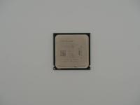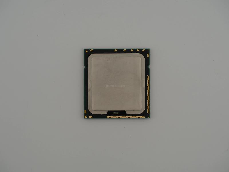
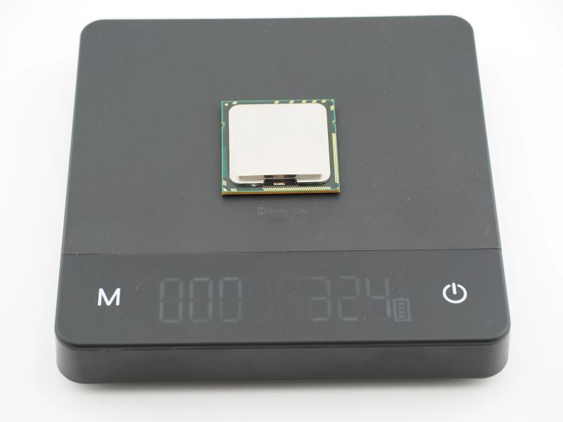
The sheer density of LGA-1366 server silicon is always striking. It sits on the scale at exactly 32.4 grams. The thick nickel-plated copper integrated heat spreader dominates the top, cleanly bonded to the green organic substrate. Looking closely under the light, the laser etching remains remarkably crisp despite its age and obvious use.
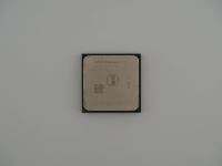
INTEL (M) (C) '09 E5620
INTEL (R) XEON (R)
SLBV4 MALAY
2.40GHZ/12M/5.86
L112B745 (e4)
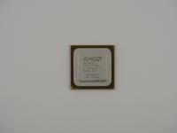
Flipping this piece over reveals the dense array of 1,366 gold-plated contact pads framing the central cavity of surface-mounted decoupling capacitors. Right in the middle of those SMDs sits a telltale marker of its modern history. A small blue and white quality control sticker is affixed across the components, bearing the letters "LQ" and the Chinese phrase "撕毁无效" indicating a voided warranty if torn. This visual clue completely changes the physical story of the chip. It is not just an enterprise processor. It is a recycled survivor.
Diving into the silicon, the E5620 represents the "tick" in Intel's classic tick-tock development model. Codenamed Westmere-EP, this is a 32-nanometer die shrink of the revolutionary Nehalem microarchitecture.
We are looking at 1.17 billion transistors packed into a 240 square millimeter die. It features four physical cores and eight threads with Intel Hyper-Threading, humming along at a base clock of 2.40 GHz. The 12M on the heat spreader denotes the generous 12 Megabytes of SmartCache shared across the cores.
The LGA-1366 platform was a massive shift in how Intel handled data. It abandoned the legacy Front Side Bus in favor of the QuickPath Interconnect (QPI). The 5.86 on the top cover indicates the QPI speed of 5.86 GT/s, allowing the CPU to communicate with the rest of the system at blistering speeds. Furthermore, the memory controller was moved directly onto the CPU die itself, supporting triple-channel DDR3 memory. This architectural leap provided massive bandwidth improvements that kept these chips relevant for years after their release. All of this compute power operates within an 80-watt Thermal Design Power rating.
To understand the Xeon E5620, you have to understand the legendary X58 motherboard platform. When Intel launched LGA-1366, it was the absolute pinnacle of high-end desktop and dual-socket server computing. Motherboards were wildly expensive, and the CPUs were equally punishing on the wallet.
The fascinating lore of the Westmere-EP Xeons lies in their afterlife. By the mid-2010s, massive enterprise datacenters began decommissioning their LGA-1366 servers. Suddenly, the secondary market was utterly flooded with cheap Xeon processors. The E5620, alongside its 6-core bigger brothers like the X5650, became the ultimate budget gamer's secret weapon.
You could buy a server chip that originally cost hundreds of dollars for the price of a fast food meal. This massive influx of cheap silicon spawned an entire cottage industry in China. Manufacturers like Huananzhi began producing brand new, highly questionable X58 clone motherboards just to give these recycled Xeons a place to live. While the E5620 was a bit overshadowed by the six-core variants in the retro-gaming community, it remained an incredibly sturdy workhorse.
Decoding the surface text tells us the exact origin of this specific unit. The S-Spec SLBV4 confirms it is the standard production stepping of the E5620. The FPO batch code L112B745 breaks down neatly. The "L" indicates fabrication at Intel's massive facility in Malaysia. The "1" designates the year 2011, and the "12" indicates the 12th week of that year. This processor was minted in late March of 2011.
The provenance story comes full circle with that blue warranty sticker on the bottom. When enterprise servers are retired, brokers buy them by the pallet. The CPUs are harvested, tested by the hundreds in massive trays in electronics markets like Huaqiangbei in Shenzhen, and then resold globally. Sellers slap these fragile paper stickers over the SMDs to prevent buyers from frying the chip by dropping it, then claiming it arrived dead. This specific chip served its time in a corporate, climate-controlled server rack for years before being yanked out, tossed in an anti-static bin, and shipped off to a new owner looking for a cheap processing upgrade. It is a perfect artifact of the global silicon recycling ecosystem.