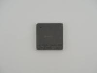
The scale clocks it in at exactly 30.4 grams, which is incredibly heavy for a processor measuring 45mm by 45mm. This heft comes from the massive metallic heat spreader brazed directly onto the substrate. The ceramic itself has that iconic, deep plum-purple hue that immediately identifies it as serious Sun Microsystems silicon.
Looking closely at the face of the artifact, the laser etching is crisp and perfectly legible. The cutouts in the metal cap are particularly fascinating, exposing the tiny surface-mount capacitors surrounding the die. Here is the exact transcription of the surface markings:
(logo) Sun
(C) (M) 1999, SMI
Ultra SPARC II
C1014583 0113
PG1.01 GS2 USA
SME 1034 LGA
980

-450
CE4
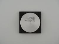
Flipping the processor over reveals an absolutely stunning grid of gold. Unlike the pin-grid arrays common to consumer desktops of the era, this is a highly advanced Land Grid Array. The pads are pristine, capturing the studio light brilliantly. A small gold triangle in the corner indicates the orientation for socketing, while the center of the grid is left devoid of pads, save for two distinct vertical columns.
This artifact represents a mature, highly refined iteration of the SPARC V9 architecture. When looking at the -450 stamping, we know this piece was binned to run at a blistering 450 MHz, pushing the physical limits of its manufacturing process.
The UltraSPARC II, code-named "Blackbird," is a 64-bit superscalar, in-order execution microprocessor. Sun engineers designed it to handle massive throughput rather than relying on deep out-of-order execution tricks. One of the most critical engineering hurdles for this chip was memory latency and cache management. The UltraSPARC II did not feature on-die L2 cache. Instead, it relied on a massive, dedicated SRAM array situated right next to the socket on the motherboard or housed within a massive processor module cartridge. This chip communicated with its external cache and the rest of the system via the proprietary Ultra Port Architecture (UPA), a highly robust interconnect designed specifically for multiprocessor scaling in heavy server environments.
The packaging itself is an engineering marvel. The SME 1034 LGA marking confirms this is a 1034-pad Land Grid Array. Using an LGA package this dense in the late 90s and early 2000s allowed Sun to ensure incredibly stable power delivery and vast amounts of I/O bandwidth to feed the processor, all while maintaining strict impedance control across the ceramic substrate.
This is the silicon that fueled the dot-com bubble. Sun Microsystems famously claimed they "put the dot in dot-com," and chips exactly like this one were the beating hearts of the Enterprise servers that ran the early internet. If you bought something online, searched a primitive database, or routed heavy enterprise traffic in 1999 or 2000, there is a very high probability an UltraSPARC II processed that transaction.
The lore surrounding these chips often centers on their thermal output and the sheer noise of the machines that housed them. Sun Enterprise servers and Ultra workstations were notoriously loud, requiring massive airflow to keep these heavy metal-capped chips from cooking themselves under sustained database loads. While Intel and AMD were fighting a brutal megahertz war in the consumer space, Sun was quietly printing money in the data center, selling reliability, unmatched multiprocessor scaling, and the rock-solid stability of the Solaris operating system.
The visual evidence on this processor leaves zero ambiguity about its identity and timeline. The copyright date reads 1999, but the batch code 0113 tells a more specific story. This exact piece of silicon rolled off the fabrication line in the 13th week of 2001. By 2001, the UltraSPARC III was already hitting the market, making this 450 MHz UltraSPARC II a late-run, highly optimized workhorse, likely destined to upgrade an existing Enterprise E4500 or power a high-end Sun Ultra 60 workstation.
The SMI designation stands for Sun Microelectronics, confirming this was packaged under Sun's direct purview. The LGA callout right on the heat spreader is a fascinating touch, almost as if the fabricator was bragging about the advanced package type. The visual condition of the gold pads on the rear suggests this chip was handled with extreme care and likely spent its life securely clamped into a production server before being safely retired to the museum archives.