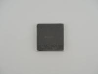
When placing this specific unit on my digital scale, it clocks in at a hefty 110.6 grams. That is a serious chunk of ceramic and silicon.
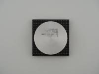
Looking at the top surface, the laser etching is faint but highly legible under the right macro lighting. I can clearly see the iconic Sun Microsystems logo with the interconnected "U"s. Here is the exact transcription of the surface text:
UltraSPARC® T1
©℗ 2005, SMI
Sun Microsystems

SME 1905A LGA     PG 2.0.1
980 USA           47313449D
86C9F4C010501
8332579181073
1000-6            DC3
527-1202-01
0829
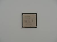
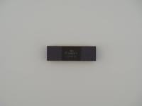
Flipping it over reveals the breathtaking LGA-1933 interface. The gold pads are arranged in a massive, dense grid with distinct cross-shaped routing channels cutting through the center. These empty avenues were necessary for signal routing and power delivery to the massive die hidden beneath the lid. The precision of the gold plating on these pads is a testament to the enterprise-grade manufacturing standards of the mid-2000s.
The UltraSPARC T1, famously known by its development codename Niagara, was an absolute beast of parallel engineering. Fabricated on a 90nm process by Texas Instruments, this piece of silicon houses roughly 300 million transistors. But it is not the transistor count that makes it special, it is how Sun chose to use them.
Instead of building a few massive, power-hungry cores with complex out-of-order execution pipelines, Sun engineers went the opposite direction. They designed an architecture meant to handle massive web traffic by focusing on thread-level parallelism. The full T1 architecture features 8 simple, in-order cores. Each core handles 4 concurrent hardware threads. That means a single CPU can juggle 32 threads simultaneously.
There is a fascinating architectural quirk to point out here. Sun realized that web servers and database transaction applications largely rely on integer math. Floating-point math is rarely used in these workloads. To save die space and power, they only included a single Floating Point Unit (FPU) on the entire chip. All cores had to share this one FPU. If you tried to run scientific simulations on this chip, it would crawl to a halt. But if you asked it to serve thousands of concurrent HTTP requests, it would absolutely destroy the competition from Intel and AMD. Furthermore, it did this while pulling a relatively modest 72 watts of power.
Sun marketed this chip under the banner of "CoolThreads" technology. It was a bold statement that directly targeted the incredibly hot and power-hungry Intel Xeon NetBurst processors of the era. The T1 was practically custom-built for the dot-com boom aftermath, where massive horizontal scaling was becoming the norm for data centers.
One of the greatest pieces of lore surrounding the UltraSPARC T1 is Sun's decision to open-source the processor's design. In 2006, Sun released the RTL (Register Transfer Level) source code under the OpenSPARC initiative. You could literally download the blueprint for this enterprise server chip, study it, and theoretically synthesize it on an FPGA if you had the hardware. It was a radical move that solidified Sun's reputation as a champion of open standards, even as their financial independence was beginning to wane.
Sadly, the T1 and its successor, the T2, were some of the last great hurrahs for Sun Microsystems before the Oracle acquisition in 2010. While Oracle continued the SPARC line for several years, the wild, experimental days of Sun hardware effectively ended, making these chips profound artifacts of computing history.
Identifying this artifact was a highly satisfying process. The UltraSPARC T1 branding is obvious, but the secondary string of numbers tells the true story of this specific piece of silicon.
As a collector, I always look for the speed grade and core count identifiers. In the center of the laser-etched block, the code 1000-6 stands out. In Sun's nomenclature for this era, this indicates a clock speed of 1000 MHz (1.0 GHz) and a 6-core configuration. While the architecture supports up to 8 cores, yield harvesting meant that chips with one or two defective cores were fused off and sold as 6-core or 4-core variants.
The Sun part number 527-1202-01 corroborates this entirely, mapping directly in vintage hardware catalogs to the 1.0 GHz 6-Core variant. Additionally, the date code 0829 in the bottom left corner is a beautiful detail. It tells me this chip was packaged in the 29th week of 2008. Even though the copyright clearly says 2005 (the year the architecture launched), this specific unit was manufactured quite late in the T1 lifecycle, right as the UltraSPARC T2 was already entering the market.