This is a massive, incredibly dense slab of enterprise computing history. When placing this artifact on my scale, it registered a hefty 239.8 grams. That is roughly half a pound of glass-ceramic, copper, and bare silicon.
Since this specific unit is missing its massive hermetically sealed cooling lid, there are no traditional part numbers or FRU codes etched onto the surface for a clean transcription.
Dimensions: 96mm x 96mm
Substrate Type: Multi-layer Glass-Ceramic
LGA Pad Count: 7,356
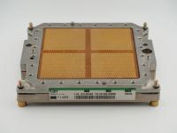
Looking closely at the top surface, notice the distinct, mottled "X" patterns etched into the thermal paste residue on every single one of the seven bare silicon dies. This pattern is a beautiful forensic remnant of the precise thermal interface application IBM used to bond the bare dies to the missing heavy metal hat. The top of the module features a central metallic standoff nub. This was engineered specifically to prevent the massive cooling assembly from crushing the delicate flip-chip silicon when clamped down.
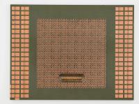
The dark brown substrate is flawless. Along the outer edges, I can see the intricate rows of surface-mounted decoupling capacitors necessary to feed clean power to the beastly dies. Flipping it over reveals an absolute sea of gold. The bottom is an LGA surface so dense it looks like woven fabric, precisely divided into four distinct quadrants. The micro-contrast of the gold pads against the dark ceramic is simply stunning.
This module is a masterclass in extreme computing density. What we are looking at is the entire beating heart of an IBM System z10 Enterprise Class mainframe.
The layout consists of seven individual dies bonded to the glass-ceramic substrate. Five of these are the CP (Central Processor) chips. Each CP chip was fabricated on a 65nm Silicon-on-Insulator (SOI) process and contains four cores, meaning this single substrate houses twenty physical mainframe cores running at a blistering 4.4 GHz.
The other two massive dies are the SC (Storage Control) chips. In the mainframe world, cache is king. These SC chips manage the massive shared Level 2 cache and act as the traffic directors for the entire system topology. To put the density into perspective, each CP die holds around 994 million transistors, and each SC die packs roughly 3.3 billion. We are looking at well over ten billion transistors operating in perfect unison on a single 96mm square.
The bottom interface is a 7,356-pad Land Grid Array. The sheer amount of mounting pressure required to make a reliable connection across over seven thousand individual pins without cracking the ceramic substrate is terrifying. The substrate itself is composed of over a hundred distinct layers of routing, designed specifically to match the thermal expansion coefficient of the silicon dies to prevent physical shearing under extreme thermal loads.
The z10 architecture was a massive inflection point for IBM. Released in 2008, it was a brutal display of brute-force engineering. While the rest of the consumer industry was backing away from the gigahertz race due to the thermal nightmare of the Pentium 4 era, IBM just leaned into the heat. They pushed their massive, complex CISC architecture to an astonishing 4.4 GHz.
The biggest architectural leap for the z10 was the introduction of out-of-order execution to the mainframe ecosystem. Prior to this, IBM z/Architecture had relied strictly on in-order pipelines. Making a fundamentally different architectural approach perfectly backwards-compatible with decades of legacy banking code was a monumental triumph.
There is a persistent myth that mainframes died out in the 1990s. Artifacts like this prove otherwise. This module was designed to process the world's credit card transactions, flight bookings, and banking ledgers with absolute zero downtime. It represents a parallel universe of computing where power consumption and cost are entirely irrelevant compared to reliability and bandwidth.
Identifying bare, unlidded mainframe modules can be tricky, but the physical layout of the silicon is a cryptographic fingerprint. I can confidently state this is an IBM System z10 EC MCM based entirely on the visual clues.
Here is the breakdown of the identification process:
The 96mm x 96mm dimensions perfectly align with the late 2000s IBM form factors. However, the exact generation is revealed by the die count.
The older z9 EC module utilized a much denser arrangement with 16 individual chips (a mix of CPs, SCs, and memory buffers). The newer z196 module, which followed the z10, utilized eight chips (six CPs and two SCs).
This specific artifact has exactly seven chips: five CPs and two SCs. That 5+2 layout is the exclusive, definitive signature of the z10 Enterprise Class MCM. Finding one of these fully intact and unbroken outside of an official IBM reclamation facility is incredibly lucky. IBM typically leases these machines and demands their total destruction upon retirement to protect intellectual property and prevent a secondary gray market. This module somehow escaped the shredder to become a crown jewel in my collection.