This specific unit is an absolute monolith of enterprise silicon. Enterprise mainframes are tightly controlled corporate assets. Finding an intact, completely naked module from this era is a serious win for any collection.
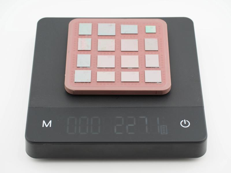
Dropping this artifact on the scale reveals a raw weight of 227.1g. We are looking at nearly half a pound of pure computing hardware with absolutely no heat sink or thermal lid attached.
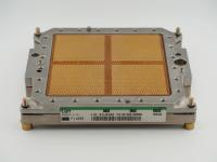
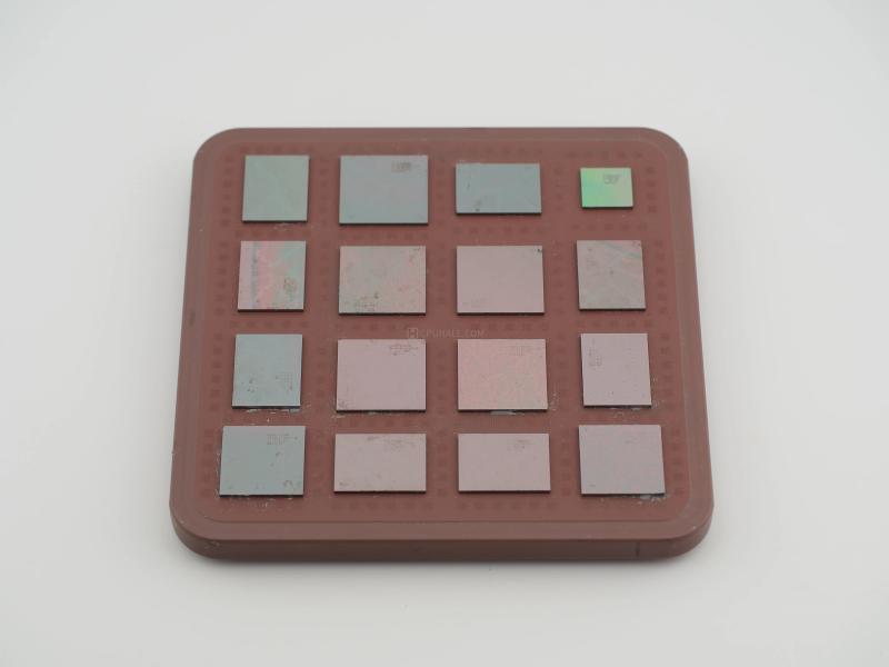
The top of the module showcases a 4x4 matrix of sixteen bare silicon dies. The ruler perfectly confirms the 96mm by 96mm physical footprint. The die arrangement is an eclectic mix of massive monolithic structures and smaller logic chips. Some dies possess a dark, almost completely opaque mirror finish, while others exhibit the iridescent green and purple refractions typical of exposed silicon.
Flipping the module over to examine the underside, I am always struck by the sheer insanity of IBM's contact grids. The bottom is saturated with a microscopic forest of gold LGA pads. These pads are physically segregated into four massive quadrants. In the dividing channels between these quadrants, we find the factory identification markings. Zooming in on, the laser-etched substrate part number FX528558 is completely pristine and highly legible. The contrast of the dark brown ceramic against the bright gold pads gives this artifact a very authoritative, cold-war-tech visual vibe.
The engineering inside this ceramic slab is nothing short of heavily weaponized mathematics. This MCM interconnects sixteen individual chips that together form the central electronic complex of an IBM System z9 node. Under full enterprise workload, this specific module package was designed to dissipate up to 1200 watts of heat. Handling that kind of thermal violence required incredibly specialized cooling solutions, which typically involved massive vapor compression refrigeration systems.
What we cannot see from the outside is just as impressive as the surface silicon. The glass-ceramic substrate acting as the foundation for these chips is actually composed of 102 individual layers. Woven inside that 96mm square footprint is approximately 0.545 kilometers of microscopic internal wiring. This vast internal network handles the insanely complex power delivery and data routing required to keep sixteen high-speed dies communicating without bottlenecking.
Operating at a clockspeed of 1.7 GHz, the processors inside this MCM utilize IBM's 64-bit z/Architecture. To an average desktop user in 2005, a 1.7 GHz clock might have sounded modest. However, mainframe processing power is derived from massive cache pools, wide memory buses, and heavily parallelized I/O subsystems rather than just raw clock frequency.
The System z9 Enterprise Class was IBM proving that vertical scaling was still very much alive. During a time when the broader tech industry was obsessing over sprawling clusters of cheap, scale-out pizza box servers, IBM doubled down on building a singular, indestructible titan.
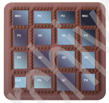
One of the greatest hardware myths from this era is that mainframes are just scaled-up desktop processors. Looking at the disparate die sizes on this MCM completely shatters that illusion. Mainframes like the z9 EC treat the CPU complex as a specialized team. There are dedicated Central Processors, specialized System Assist Processors strictly for handling I/O, and massive off-die System Cache pools. This architecture ensured that the main compute cores never had to wait on data retrieval. It is a completely different philosophy of hardware design.
Identifying naked IBM substrates can sometimes feel like reading tea leaves, but the visual evidence here makes for a very confident classification. The die sizes and the specific physical layout of the sixteen chips on this 96mm substrate confirm this is an IBM System z9 EC module.
The predecessor to this architecture, the z990 (code-named T-Rex), utilized a visibly different die layout and substrate design. Furthermore, the successor architecture (the z10 EC) completely redesigned the silicon to push clockspeeds up to 4.4 GHz. The physical measurements of the processor units and cache dies seen perfectly align with the 1.7 GHz z9 EC generation.