Weighing in at exactly 23.1 grams on the scale, this specific unit feels substantial in the hand.
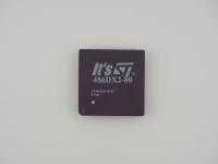
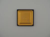
The top surface is remarkably clean, featuring a crisp white laser etching alongside a beautiful, holographic Windows compatibility sticker that absolutely screams mid-90s multimedia PC.
Here is the exact transcription of the top markings:
TEXAS INSTRUMENTS
486DX2-80
TI486DX2-G80-GA
VCC=3.45V
FOR OEM USE ONLY
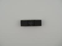
Flipping the artifact over reveals the central black epoxy block covering the die cavity, framed by an immaculate grid of staggered gold pins. The macro lens captures the faint, slightly degraded laser etching on the bottom:
4085977-0003
TAIWAN
CB0-58CFEDT
The physical condition is excellent. The pins are straight and the ceramic shows virtually no chipping along the edges. The FOR OEM USE ONLY designation gives it a nice corporate flavor, indicating this piece was originally destined for the bowels of a pre-built desktop from a major vendor rather than a shiny retail box.
To understand this chip, we have to look past the Texas Instruments logo and recognize the Cyrix engineering underneath. This is a Cyrix Cx486DX2 core fabricated by TI. At the time, Cyrix lacked their own semiconductor fabrication plants. They operated as a fabless design house and partnered with manufacturing giants like SGS-Thomson and Texas Instruments to physically produce their silicon. In exchange for manufacturing the chips, TI was granted the rights to sell these Cyrix designs under their own brand name.
Technically, this is a very interesting piece of the 486 puzzle. The DX2 moniker means it uses a clock multiplier of two. It runs internally at 80 MHz while communicating with the motherboard over a 40 MHz front-side bus. Pushing the bus to 40 MHz was a hallmark of AMD and Cyrix boards, whereas Intel largely preferred the safer 33 MHz bus multiplied up to 66 MHz for their classic DX2-66.
Crucially, the front clearly states VCC=3.45V. Early 486 processors were massive heat generators that required a full 5 volts. By moving to a 3.45V logic level, this chip ran significantly cooler and consumed less power. This meant you could not simply drop it into an older Socket 1 or Socket 2 motherboard without a voltage regulator module, but it was perfectly at home in a late-era Socket 3 board. It features an 8KB internal write-back cache, which gave it a respectable Instructions Per Clock advantage in everyday integer workloads compared to early Intel steppings.
This artifact represents the absolute peak of the great 486 Clone Wars. In 1994, Intel was desperately trying to convince the computing world to abandon the 486 architecture and upgrade to their expensive new Pentium platform. However, the rest of the industry rebelled. Companies like AMD, Cyrix, and IBM saw massive consumer demand for fast, cheap upgrades that fit into existing 486 motherboards.
The TI 486DX2-80 is a testament to that rebellion. It provided a cheap upgrade path that allowed budget-conscious consumers to squeeze a few more years out of their aging rigs. There is a persistent myth that these Cyrix-designed chips ran absurdly hot and crashed constantly. In reality, the stability issues were almost always caused by users dropping these 3.45V parts into older 5V motherboards without proper voltage regulation, or by cheap motherboards failing to handle the aggressive 40 MHz front-side bus. When properly configured on a quality Socket 3 board, this chip was a rock-solid workhorse.
The inclusion of the Windows sticker right on the ceramic is a fun piece of lore. Microsoft was pushing Windows 3.1 and early Windows 95 builds aggressively, and hardware manufacturers paid a premium to slap that logo on their components to guarantee compatibility to nervous buyers. It is a brilliant piece of marketing permanently fused to the silicon.
Identifying this specific unit is incredibly straightforward thanks to the pristine top markings. The TI486DX2-G80-GA string tells us everything we need to know. The G80 firmly establishes the 80 MHz clock speed, while the GA stepping points to a later revision of the manufacturing process that optimized the 3.45V thermal envelope.
The FOR OEM USE ONLY text is the real provenance clue here. Texas Instruments sold massive trays of these chips to companies like Acer, AST, and Packard Bell. Because it lacks a retail heatsink or retail packaging, it is highly likely this chip spent its active life inside a beige, heavy steel desktop case in a corporate office or a family computer room before finally being rescued and placed into my collection. The bottom markings CB0-58CFEDT are typical TI batch and fab tracking numbers from their Taiwan facilities, confirming the origin of the physical silicon.