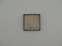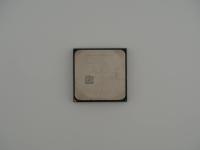
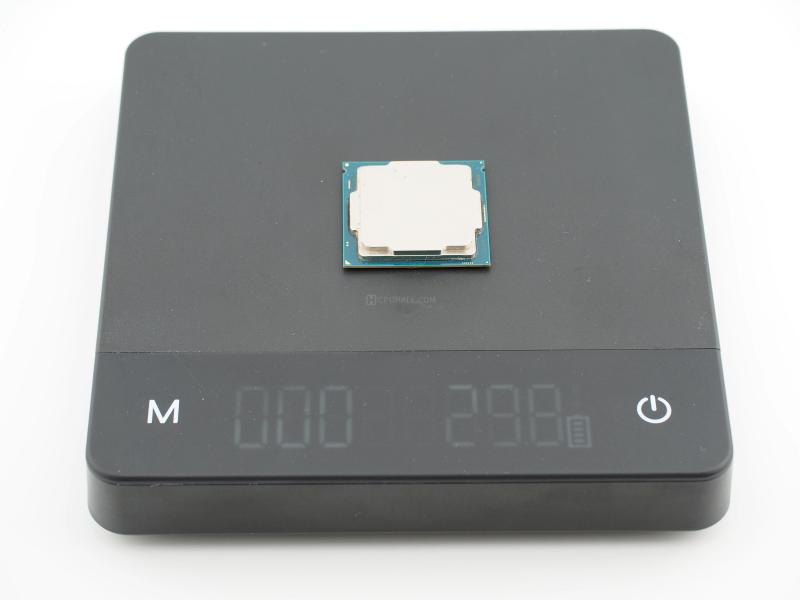
Holding this piece and throwing it on the digital scale, it clocks in at exactly 29.8 grams. It is a dense little square of modern manufacturing. Looking at the macro shots of the Integrated Heat Spreader (IHS), the laser etching is clear but shows the unmistakable faint scuffs and thermal paste ghosting of a chip that has been socketed and put to work.
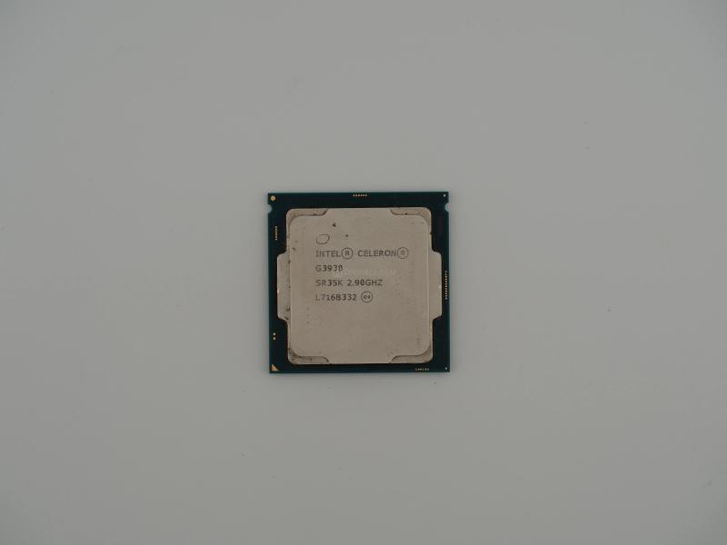
Here is the exact surface text transcribed from the nickel-plated copper:
INTEL (R) CELERON (R)
G3930
SR35K 2.90GHZ
L716B332 e4
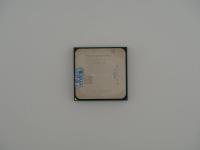
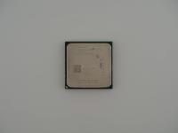
Flipping the silicon over, we see the classic LGA-1151 pad layout. The gold pads are immaculate. In the central cavity of the fiberglass substrate, there is a very sparse arrangement of tiny Surface Mount Device (SMD) capacitors. Compared to high-end Core i7s of the same generation which have this cavity absolutely packed to the brim with power delivery components, the barren layout here physically represents how little power this die actually demands. Sizing it up against the millimeter ruler, it strictly conforms to the standard 37.5mm by 37.5mm package dimensions.
From an engineering perspective, there is no heavy metal thunder here. This is bare-bones computing. Underneath that metal lid sits a piece of 14nm+ silicon based on the Kaby Lake microarchitecture. Intel brutally segmented this chip to hit a rock-bottom price point. It features only two physical cores, absolutely zero hyperthreading, and a meager 2MB of L3 cache.
While flagship chips of this era were pushing thermal limits, the G3930 sips power with a Thermal Design Power (TDP) of just 51 watts. In reality, under typical loads, it barely touches a fraction of that. The internal graphics processor is the highly castrated Intel HD Graphics 610. It lacks the execution units to do anything visually impressive, but it handles basic display outputs perfectly fine. The engineering triumph of this chip is not its speed, but the sheer yield and scale at which Intel could manufacture them flawlessly.
Here is where this seemingly boring piece of fiberglass gets genuinely interesting. If we are talking desktop computing history, the Celeron G3930 is a footnote. But if we are talking the history of cryptocurrency, it is a legend.
During the massive Ethereum mining boom of 2017, miners were buying up high-end graphics cards by the pallet. To run six, eight, or even nineteen GPUs on a single motherboard, you needed a CPU. But mining algorithms run almost entirely in the video card's memory. The main system processor literally just needs to boot Windows or Linux and manage PCIe lanes. Miners realized they were burning money buying Core i3 or i5 processors.
Enter the G3930. Because it was the absolute cheapest LGA-1151 processor you could buy brand new (often retailing around $40 USD), it became the heart of millions of mining rigs around the world. There were times during 2017 and 2018 where you could not find this bottom-tier processor in stock anywhere because mining farms were absorbing the entire global supply chain. It is hilarious to think about this hyper-budget dual-core CPU sitting at the center of rigs generating tens of thousands of dollars in digital currency.
There is no mystery to solve with this specific artifact. I can confidently decode its exact origins just by reading the batch code L716B332.
The L indicates it was fabricated and packaged at Intel's assembly plant in Malaysia. The 7 tells us the year is 2017. The 16 means it rolled off the line in the 16th week of the year (roughly mid-April). The B332 is the specific lot tracking number. The SR35K S-Spec strictly identifies it as the Kaby Lake dual-core stepping. Everything about this chip aligns perfectly with the timeframe of the great mining rush. It is a perfect, mass-produced specimen of late-2010s budget silicon.