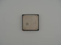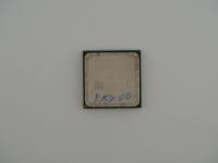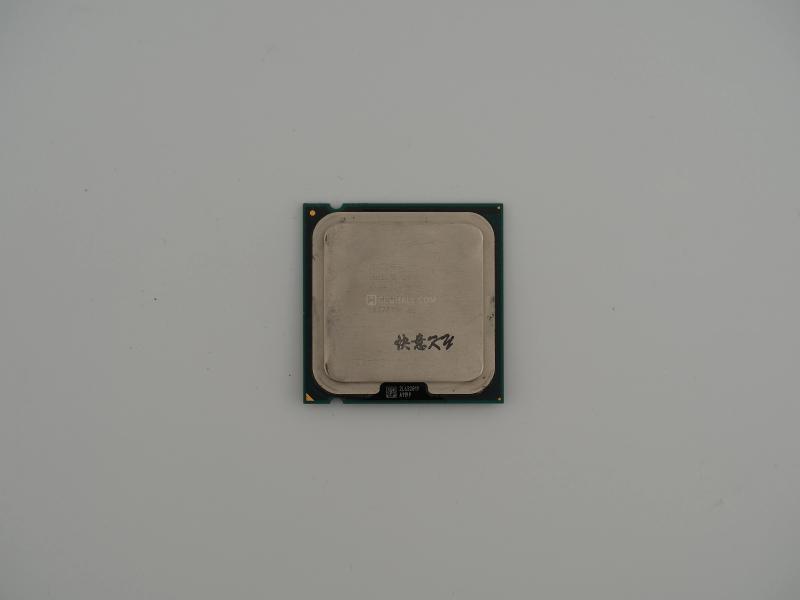
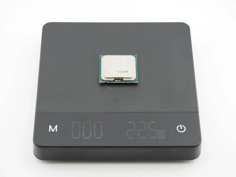
It tips the scales at exactly 22.5 grams. The top features the familiar, slightly dull luster of a nickel-plated copper integrated heat spreader (IHS), while the underside presents the dense grid of gold contact pads characteristic of Socket T.
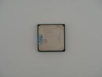
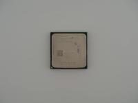
INTEL (M) (C) '05
INTEL(R) CORE(TM)2 DUO
6600 SL9S8 MALAY
2.40GHZ/4M/1066/06
L632A486 (e4)
The physical condition tells a story of heavy use. There are minor clamping marks on the edges of the IHS from where the motherboard socket mechanism locked it down. The bottom shows the standard array of tiny surface-mount capacitors sitting right in the center of the LGA pad array. What gives this specific artifact a bit of unique charm is the black permanent marker scrawled right over the Intel logo. It reads roughly as "快意" followed by a stylized number that appears to denote its 2.4 GHz clockspeed. This is a classic hallmark of the Asian second-hand hardware market, where vendors rapidly test and bin trays of recycled CPUs, marking them for quick sorting.
Diving into the technical specifications of the E6600, we are looking at the legendary Conroe core. Fabricated on Intel's 65nm process node, this die packs 291 million transistors.
The architecture inside this unassuming package was a total paradigm shift. Intel had pushed their NetBurst architecture to its absolute thermal and frequency limits with the Pentium 4 and Pentium D. Those chips ran absurdly hot and featured incredibly long, inefficient 31-stage pipelines. The Core microarchitecture featured here took a different path. Designed by Intel's team in Haifa, Israel, it borrowed heavily from the power-efficient Pentium M mobile processors.
This chip features a 14-stage pipeline and a wide dynamic execution engine capable of issuing four instructions per clock cycle. The defining feature of the E6600 is its massive 4MB of shared L2 cache. At the time, allowing both execution cores to dynamically share the entire pool of L2 cache was a brilliant engineering move that drastically reduced cache misses and memory latency. It operates on a 1066 MHz Front Side Bus (FSB) and has a Thermal Design Power (TDP) of just 65 watts. Compared to the fiery 130-watt monsters it replaced, the Conroe ran remarkably cool.
You cannot talk about CPU history without talking about the summer of 2006. Prior to Conroe, AMD was completely dominating the enthusiast and gaming markets with their Athlon 64 and Athlon 64 X2 processors. Intel was bleeding market share and looking completely lost, trying to convince the world that gigahertz mattered more than actual instructions per clock.
When the Core 2 Duo launched in July 2006, it was an absolute massacre. The E6600 was the undisputed sweet spot of the lineup. Priced aggressively at around $316 at launch, it absolutely obliterated AMD's flagship processors that cost over twice as much. It was cooler, it was vastly faster, and it possessed an almost mythical capacity for overclocking.
Hardware enthusiasts quickly discovered that the E6600 was practically begging to be pushed. Because of its relatively low 9x multiplier and the robust nature of the 65nm silicon, overclockers were routinely taking this 2.4 GHz chip well past 3.0 GHz, and often up to 3.6 GHz on standard air cooling. It became the defining gamer CPU of its era. This chip single-handedly restored Intel's absolute dominance in the desktop market, a crown they would hold largely uncontested until the arrival of AMD's Ryzen over a decade later.
Because of the sheer volume of Core 2 Duo processors manufactured, pinpointing the exact life cycle of this specific artifact is impossible, but the codes tell us exactly where and when it was born.
The SL9S8 S-Spec confirms this is a B2 stepping of the Conroe core. The batch number L632A486 breaks down nicely. The "L" signifies it was manufactured in Malaysia. The "6" gives us the year 2006, and "32" indicates it was fabbed in the 32nd week of that year, placing its birth in mid-August 2006. This means it was part of the very first wave of Conroe chips to flood the market right after the July launch. The (e4) mark indicates compliance with RoHS regulations, meaning the package uses lead-free solder.
I acquired this piece exactly as you see it. The vendor marks heavily imply it spent years crunching numbers in a corporate office or a massive internet cafe in Asia before the entire system was decommissioned, stripped for parts, and the CPU was thrown into an anti-static tray with hundreds of its brothers. It lacks the aesthetic prestige of a gold-capped ceramic mainframe chip, but in terms of pure historical impact, the silicon under this lid changed the computing landscape overnight.