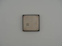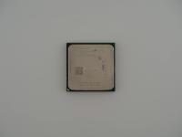
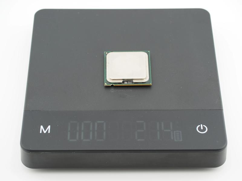
Holding this piece of hardware and placing it on the scale, it registers a satisfying 21.4 grams. This weight comes entirely from the thick nickel-plated copper Integrated Heat Spreader (IHS) and the dense fiberglass substrate. When looking closely at the top of this artifact, the surface shows the telltale swirl of light scuffs from years of thermal paste application and the clamping force of heavy aftermarket coolers.
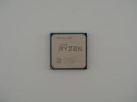
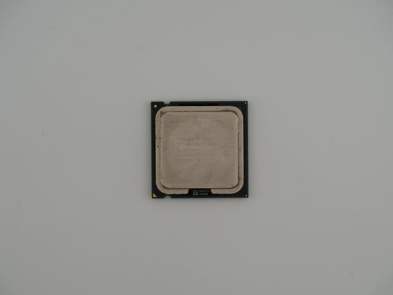
The laser etching on the IHS is highly legible and provides a perfect forensic roadmap to this chip's origins. Here is the exact transcription of the top markings:
INTEL (M) (C) '06 Q8200
INTEL (R) CORE(TM)2 QUAD
SLG9S MALAY
2.33GHZ/4M/1333/05A
L851B276 (e4)
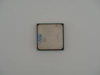
Flipping the chip over reveals the classic 775 gold contact pads. The array is interrupted in the center by a cluster of surface-mounted decoupling capacitors. On the bottom right edge of the green PCB, the original fab part numbers N384412 and 6A4546 are clearly visible. The L851B276 batch code on the front tells me everything I need to know about its birth. It was manufactured in Malaysia during the 51st week of 2008.
Diving into the technical architecture of the Q8200, we are looking at the Yorkfield core. This is built on Intel's incredibly successful 45nm manufacturing process using high-k metal gate technology. What makes this processor fascinating is that it is not a monolithic quad-core chip. Underneath that copper heat spreader, there are two separate 45nm Wolfdale dual-core dies sitting side-by-side on the same package, communicating over the Front Side Bus.
This specific unit runs at a 2.33 GHz clockspeed across a 1333 MHz Front Side Bus. The 4M in the string denotes the L2 cache, which is split evenly between the two dies at 2MB per dual-core block. Intel aggressively binned and laser-cut this silicon to hit a specific price point, slashing the cache down from the massive 12MB found on the flagship Q9000 series parts. Despite the cutbacks, it still packed 820 million transistors into a 95W Thermal Design Power envelope.
The Core 2 Quad series represents a brutal turning point in the legendary Intel versus AMD rivalry. During this era, AMD boldly claimed that true quad-core processors needed to be a single piece of silicon natively designed with four cores. Intel ignored that philosophy entirely. They essentially glued two dual-core processors together and shipped them. The joke in the industry was that Intel's "glued" processors absolutely decimated AMD's native quad-core Phenom lineup in almost every benchmark.
The Q8200 was introduced in late 2008 as the absolute cheapest way to get an Intel quad-core into a desktop machine. It was a massive commercial success because it allowed budget builders and OEM companies like Dell and HP to slap a "Quad Core" sticker on their boxes without paying the premium commanded by the Q6600 or the Q9550. Overclockers, however, generally hated this specific chip. The low multiplier of 7x combined with a high stock Front Side Bus meant pushing it past 2.8 GHz required an incredibly expensive motherboard capable of handling extreme bus speeds.
The provenance of this specific unit is crystal clear. The high-resolution imagery leaves absolutely no room for mystery. The SLG9S S-Spec confirms this is a Yorkfield stepping R0 chip. The R0 stepping was the final and most refined silicon revision for the Yorkfield family, adding a few minor power management instructions (XSAVE and XRSTOR) that previous steppings lacked. The 2006 copyright date on the heat spreader throws a lot of novice collectors off, but that year simply refers to when Intel registered the copyright for the Core 2 Quad branding, not when the silicon was actually pressed.