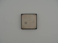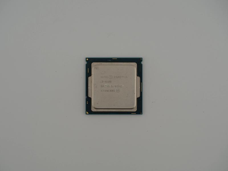
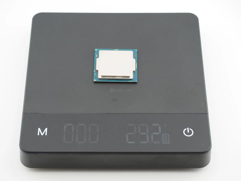
Placing this piece on the scale, it weighs in at exactly 29.2 grams of silicon, copper, and fiberglass. Measuring roughly 37.5mm square, this artifact represents the peak of mainstream consumer electronics from the mid-2010s. Looking closely at the top of the nickel-plated copper integrated heat spreader (IHS), the laser etching is remarkably crisp, cutting through the matte gray surface to reveal the following telemetry:
INTEL (R) CORE (TM) i3
i3-6100
SR2HG 3.70GHZ
X749C685 (e4)
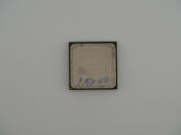
Flipping this artifact over reveals the LGA-1151 contact pad array. There are no delicate gold pins here to bend or break, just a sea of perfectly uniform gold-plated lands surrounding a densely packed central array of surface-mount capacitors. The PCB itself is a standard green fiberglass substrate. It lacks the exotic, heavy ceramic feel of the mainframe chips in the collection, but it possesses a sterile, highly engineered precision that is objectively impressive.
Underneath that heat spreader lies the Skylake architecture, fabricated on Intel's heavily refined 14nm process node. This is a dual-core processor with Hyper-Threading enabled, allowing it to juggle four threads simultaneously. While that sounds paltry by today's standards, back in 2015, this was a highly efficient compute engine with a base clock of 3.7 GHz and a surprisingly low Thermal Design Power (TDP) of just 51 watts.
Skylake was a massive architectural shift for Intel. They ripped the Fully Integrated Voltage Regulator (FIVR) out of the CPU package and pushed that responsibility back onto the motherboard. This made the chips inherently cooler than their Haswell predecessors. It also marked the mainstream transition to DDR4 memory, featuring a dual-channel memory controller that could officially handle DDR4-2133 or DDR3L-1600. Integrated into the silicon die is the Intel HD Graphics 530 engine, which took up a significant portion of the total transistor budget. It was not meant for heavy lifting, but it could decode 4K video streams without breaking a sweat.
On paper, the Core i3-6100 was just another locked, budget-tier processor destined for office PCs and cheap gaming rigs. Intel's strict segmentation rules dictated that only processors with a "K" suffix (like the i5-6600K or i7-6700K) were allowed to be overclocked.
However, hardware enthusiasts are a stubborn breed.
Shortly after Skylake launched, a massive exploit was discovered. Motherboard vendors accidentally (or perhaps intentionally) released BIOS updates for their high-end Z170 boards that unlocked the Base Clock (BCLK) for non-K processors. Because Skylake decoupled the PCIe and DMI buses from the base clock, you could suddenly crank the BCLK through the roof without crashing your storage drives or graphics card.
Overnight, this humble $117 chip became a legend. Enthusiasts were pushing the i3-6100 from its stock 3.7 GHz to an absolutely screaming 4.5 GHz or higher on standard air coolers. It was cannibalizing sales of much more expensive i5 processors because a heavily overclocked i3-6100 could match them in single-threaded gaming performance. Intel was furious and eventually forced motherboard partners to issue microcode updates to lock the exploit down. But for a brief, glorious window, this exact model of chip was the undisputed king of rebel overclocking.
I do not need to guess much about this specific unit. The visual evidence is overwhelmingly conclusive. The S-Spec SR2HG perfectly identifies this as a retail stepping (R0) Core i3-6100.
Decoding the batch number (FPO) X749C685 tells us the origin story of this exact piece of silicon. The "X" prefix indicates it was fabricated and packaged at Intel's assembly plant in Vietnam. The subsequent digits suggest a late 2017 manufacturing date, which makes sense as Skylake parts were produced for years after their initial release to satisfy OEM demand. It is a mass-market chip, entirely devoid of the exotic rarity found in Soviet clones or prototype ceramic modules. Yet, having it in the museum is essential. It serves as a perfect physical anchor point for the history of 14nm consumer silicon and the infamous non-K overclocking saga of 2015.