This specific unit weighs exactly 30.0 grams on my scale and measures just under 38 millimeters across.
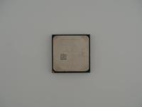
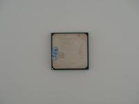
Looking closely at the Integrated Heat Spreader (IHS), the laser etching is highly legible despite some residual thermal paste caked around the lower edges. We have some aftermarket graffiti here too. Someone has hastily scribbled "A.1" and what looks like "2004" or some other cryptic inventory code in blue permanent marker right across the Intel logo.
Here is the exact transcription of the laser etching pulled directly from the metal:
INTEL (R) CORE(TM) i3
i3-7100
SR35C 3.90GHZ
X809D115 (e4)
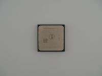
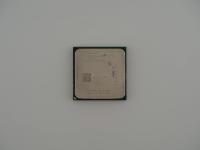
Flipping the chip over reveals the classic LGA-1151 pad arrangement. The 1,151 gold-plated contact pads are in good condition without any obvious burns or physical gouges. The central cavity houses a densely packed array of tiny surface-mount capacitors (SMDs) necessary for power delivery smoothing. The aesthetic is clean and ruthlessly optimized for mass manufacturing.
The Core i3-7100 represents the seventh generation of Intel's Core series, codenamed Kaby Lake. Beneath the nickel-plated copper heat spreader lies a die built on Intel's 14nm+ fabrication node. This was the era when Intel essentially perfected their 14-nanometer process to squeeze every last drop of frequency out of the silicon.
Technically speaking, this processor features 2 physical cores and 4 threads thanks to Hyper-Threading. It runs at a locked base clock of 3.90 GHz and does not support Intel Turbo Boost technology. The thermal design power (TDP) is a very mild 51 watts, meaning this chip could easily be kept cool by the notoriously flimsy Intel stock cooler.
The architecture itself is virtually identical to the previous Skylake generation. The engineering triumph of Kaby Lake was not a dramatic IPC (Instructions Per Clock) uplift, but rather a refinement of the transistors themselves. They optimized the fin profile and pitch of their 14nm process to allow for higher clockspeeds at the same voltage. The chip also features integrated Intel HD Graphics 630, which included an updated media engine capable of hardware decoding 10-bit HEVC and VP9 video. This made the i3-7100 an absolute favorite for basic office workstations and home media servers.
In the grand halls of CPU history, the i3-7100 occupies a fascinating, somewhat tragic position. It was released in early 2017. At the time, an entry-level dual-core processor with four threads was completely standard. For years, Intel had dictated that the i3 got two cores, the i5 got four cores without Hyper-Threading, and the i7 got four cores with Hyper-Threading.
The i3-7100 is a perfect physical artifact of Intel's absolute complacency right before the storm hit. Just months after this chip hit the market, AMD launched their Ryzen architecture. The industry paradigm shifted overnight. Suddenly, dual-core desktop processors were functionally obsolete. Intel panicked and rushed their 8th generation Coffee Lake processors out the door later that same year, forcefully upgrading the i3 tier to four true physical cores.
Because of this brutal market timing, the i3-7100 and its Kaby Lake siblings aged faster than almost any other CPU generation in modern history. The myth at the time was that Kaby Lake was a massive architectural leap, but hardware enthusiasts knew it was merely a stopgap. Looking at this artifact, I see the very end of the dual-core desktop era. It is a monument to the calm before the Ryzen revolution.
There is no great mystery regarding the identity of this silicon. The laser markings are definitive. The S-Spec SR35C perfectly matches the retail stepping for the Core i3-7100.
The batch code X809D115 tells us exactly where and when this specific piece of silicon was born. In Intel's coding scheme, the first letter represents the fabrication or assembly plant. The "X" indicates the processor was assembled in Vietnam. The next digit "8" signifies the year 2018, and "09" indicates the 9th week of that year. Therefore, this exact chip was packaged in late February or early March of 2018.
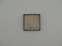
The blue marker writing on the IHS strongly suggests this chip was pulled from a corporate fleet machine or a school laboratory. IT departments frequently mark inventory numbers directly on the heat spreader when decommissioning or cataloging parts. It is a common, reliable workhorse that likely spent its life grinding through spreadsheets and browser tabs before being harvested for the secondary market.