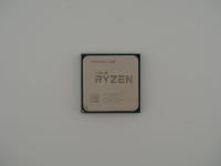
Weighing it on my digital scale gives a very standard mass of 30.4 grams for modern desktop silicon, largely dictated by the thick nickel-plated copper Integrated Heat Spreader resting on top. Measuring it against the ruler, we see the standard 37.5mm by 37.5mm dimensions that Intel relied on for several socket generations.
Looking closely at the surface of this specific unit, I can see the residual dust and faint thermal paste crust along the stepped edges of the IHS. It tells a story of a chip that lived its life under a cooler, likely grinding away in an office machine or a budget gaming rig.
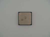
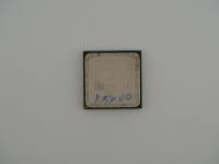
INTEL(R) CORE(TM) i3
i3-8100
SR3N5 3.60GHZ
X840D869 (e4)
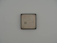
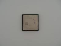
Flipping it over to inspect the LGA-1151 pad array reveals the classic dense grid of gold contact pads. The central cavity is populated with microscopic Surface Mount Device capacitors, crucial for smoothing out the power delivery before it hits the die.
Underneath that metal lid lies the Coffee Lake architecture. Built on Intel's highly refined 14nm++ process node, this chip represents a massive leap in multi-core performance for the entry level market. Prior to this generation, the Core i3 badge was strictly a dual-core affair, sometimes with hyper-threading to fake a quad-core experience. The i3-8100 features four physical, dedicated cores. It completely lacks hyper-threading, offering four threads total, but the jump in raw IPC and physical core count was massive.
It operates at a base clock of 3.60 GHz with no turbo boost capability, keeping thermals well within a very manageable 65W TDP. On the silicon, Intel also packed in 6MB of L3 Smart Cache and their UHD Graphics 630 integrated GPU. That integrated graphics block was a lifesaver for corporate desktops, allowing the system to run displays without needing a dedicated graphics card.
The physical interface is where things get controversial. It uses the LGA-1151 socket, exactly like the previous Skylake and Kaby Lake generations. However, Intel subtly rearranged the power delivery pins. This meant this Coffee Lake chip required a brand new 300-series motherboard chipset to boot.
The history of the i3-8100 cannot be told without mentioning AMD. For the better part of a decade, Intel was entirely comfortable sitting on a stagnant product stack. An i3 had two cores. An i5 had four cores. An i7 had four cores with hyper-threading. The formula never changed.
Then AMD released the first generation of Ryzen.
Ryzen completely upended the core-count hierarchy. Suddenly, budget AMD chips were packing four or even six cores. Intel went into full panic mode. The Coffee Lake generation was their aggressive, reactionary counter-punch. To stay competitive, Intel had to push their entire product stack up a tier. The i3-8100 became a true quad-core processor, effectively making the previous generation's Core i5 obsolete overnight for a fraction of the cost.
The lore surrounding this chip mostly revolves around the socket controversy. Intel claimed the older 100 and 200 series motherboards lacked the robust power delivery required for the new Coffee Lake chips. The hardware community naturally took this as a challenge. Modders quickly figured out how to isolate specific pins with tape and flash custom BIOS files, successfully booting chips exactly like this i3-8100 on older Z170 and Z270 motherboards. It proved that Intel's hard lockout was at least partially driven by a desire to sell new motherboards, earning them a fair bit of community backlash.
Identifying modern Intel silicon is thankfully a straightforward forensic exercise compared to my older cold war prototypes. The surface text gives us everything we need. The S-Spec code SR3N5 definitively locks this in as the retail stepping of the Core i3-8100.
The most interesting part of the etching is the batch code, known technically as the FPO (Finished Process Order). By decoding the string X840D869, we can pinpoint exactly where and when this piece of silicon was born.
The first character X indicates the fabrication and assembly plant. In Intel's internal tracking, "X" points to their massive facility in Vietnam. The next digit 8 denotes the year of manufacture, meaning 2018. The following two digits 40 indicate the week of that year. Therefore, I can confidently say this specific CPU was packaged in Vietnam during the first week of October 2018. The final (e4) marking in the corner indicates the chip complies with RoHS environmental standards for lead-free solder finishes. It is a perfectly documented, textbook example of late 2010s semiconductor manufacturing.