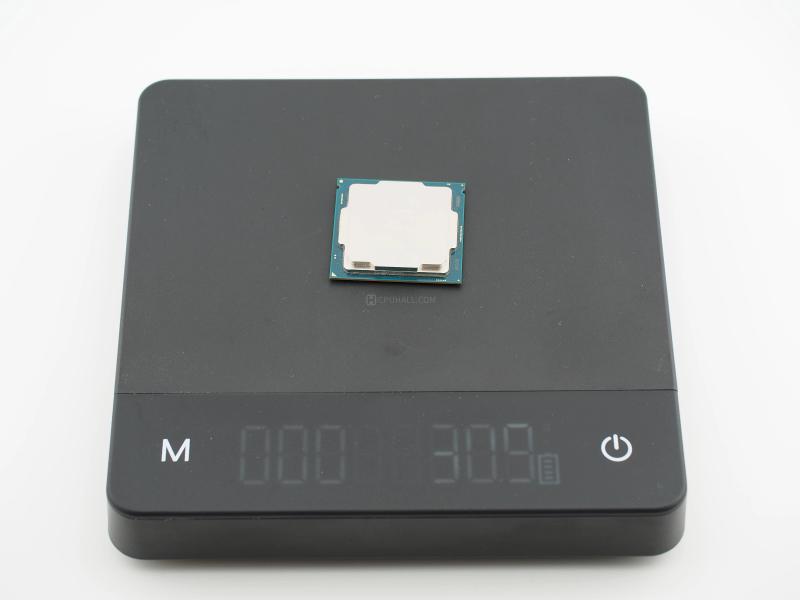
It registers precisely at 30.9 grams. The weight is almost entirely in the thick nickel plated copper integrated heat spreader (IHS) sitting atop the thin fiberglass substrate.
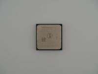
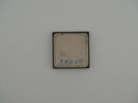
Under the lens, the surface text is sharply burned into the metal without any fading.
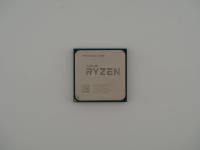
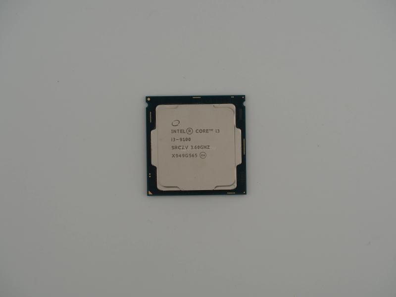
INTEL (R) CORE (TM) i3
i3-9100
SRCZV 3.60GHZ
X949G565 (e4)
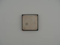
Flipping this piece over reveals the standard 1151 gold plated contact pads. The central array of surface mounted capacitors is pristine. The edges of the green PCB show the familiar semi-circular alignment notches that prevented system builders from dropping these into older, electrically incompatible motherboards.
This chip represents the zenith of Intel's highly refined 14nm++ manufacturing process. The Coffee Lake architecture was a direct response to a shifting market. Inside this package is a monolithic die packing four physical cores and four threads. Intel stripped away hyperthreading for the i3 tier in this generation, relying purely on raw IPC and high clock speeds to drive performance.
The thermal density here is manageable. With a base clock of 3.6 GHz and a maximum turbo frequency pushing up to 4.2 GHz, it carries a modest 65W TDP. The (e4) marking on the IHS indicates the use of lead free solder, though in this specific tier, Intel reverted to using standard thermal paste between the silicon die and the IHS rather than the liquid metal solder found on their high end Core i9 chips of the same era.
The LGA-1151 form factor here is specifically the "v2" or 300-series revision. While it physically shares the exact same pin count as the older Skylake and Kaby Lake sockets, Intel radically changed the power delivery pinout. Dropping this processor into an older Z170 motherboard would do nothing but spin the fans.
The Core i3-9100 is a fascinating artifact purely because of the market dynamics that forced it into existence. For nearly a decade, the "Core i3" moniker meant a strict dual core processor with hyperthreading. It was the standard office PC chip.
Then AMD released the Ryzen architecture. Suddenly, dual cores were obsolete.
Intel panicked in the best possible way for consumers. By the 8th and 9th generations, they shifted their entire stack. The i3 became a true quad core. Sitting on a shelf, this humble i3-9100 effectively matches the performance of an older 7th generation Core i5 flagship. This was a massive architectural trickle down. The 9100 became the undisputed king of budget gaming rigs in 2019. It paired beautifully with cheap graphics cards and provided exceptional single core performance for esports titles.
There is a running joke in the hardware community about Intel's "14nm++++++" era. This chip lived right in the middle of it. Intel could not get their 10nm process to yield properly, so they just kept refining 14nm over and over. The 9100 is the brute force result of a company refining a mature node to its absolute physical limit.
There is no mystery regarding the identity of this silicon. The laser etching is a direct map to Intel's production logs. The S-Spec SRCZV perfectly identifies this as the B0 stepping of the i3-9100, which includes the Intel UHD Graphics 630 silicon active on the die.
The batch code X949G565 tells the rest of the story. The "X" prefix designates that this specific wafer was processed and packaged at Intel's facility in Vietnam. The "949" indicates it was manufactured in 2019 during the 49th week of the year. This piece was rolling off the assembly line right as the world was about to shut down in early 2020.
It is a remarkably common chip, but having it documented with macro photography preserves a snapshot of what standard consumer compute power looked like at the very end of the 2010s.