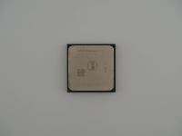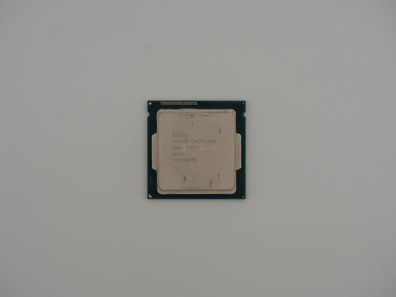
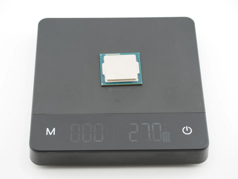
At exactly 27.0 grams, it feels dense and familiar in the hand. Dropping it next to a ruler confirms the standard 37.5mm by 37.5mm dimensions characteristic of Intel's mainstream desktop packages of the era. The surface etching on the nickel-plated copper Integrated Heat Spreader is wonderfully crisp in these macro photographs.
Looking closely at the metal under the light, the laser-etched topography tells us exactly what we are dealing with:
i(M)(C)11
INTEL(R) CORE(TM) i5-4590
SR1QJ 3.30GHZ
MALAY
L415C558 (e4)
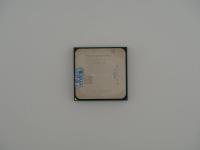
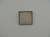
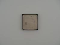
Flipping the artifact over reveals the 1,150 gold-plated contact pads. The array is perfectly preserved with no visible oxidation. In the central cavity on the underside, we see the intricate cluster of surface-mounted decoupling capacitors necessary to feed clean power to the die above. The small 200 printed on the PCB routing just below the center array is a nice touch of manufacturing transparency.
This piece represents the heart of the Haswell architecture. Built on Intel's highly mature 22nm fabrication node featuring Tri-Gate 3D transistors, the Core i5-4590 is a true quad-core processor lacking Hyper-Threading. It shipped with 6MB of L3 cache and a base clock of 3.30 GHz, capable of boosting up to 3.70 GHz when thermals allowed.
From a purely technical standpoint, Haswell was an incredibly ambitious undertaking. The most fascinating engineering quirk of this specific generation was Intel's decision to move the voltage regulator off the motherboard and directly onto the CPU package. This Fully Integrated Voltage Regulator (FIVR) gave the chip unprecedented granular control over its own power states, allowing it to drop power consumption to near zero when idling.
However, this innovation came with a brutal physical cost. Moving the voltage regulation directly beneath the Integrated Heat Spreader meant the chip generated concentrated, localized heat. The 84W Thermal Design Power rating felt much hotter in practice. Combined with Intel's controversial decision to use standard thermal paste instead of fluxless solder between the silicon die and the heat spreader, these processors demanded serious aftermarket cooling if pushed hard.
This is the processor that simply refused to die.
Sitting right in the middle of Intel's "tick-tock" cadence stagnation, the Core i5-4590 was released during an era where AMD's FX series was failing to compete on single-thread performance. Intel had absolutely no reason to push core counts past four for the mainstream consumer. Because of this lack of competition, software developers and game studios optimized heavily for four cores and four threads. As a result, anyone who bought this exact chip in 2014 could comfortably run top-tier games and applications all the way up until 2020.
There is a running joke in hardware circles that Haswell i5 processors are the cockroaches of the silicon world. They survived three different console generations, endless Windows updates, and massive shifts in GPU power. The FIVR technology that made this chip so unique was actually abandoned by Intel just two generations later in Skylake because of the thermal headaches it caused motherboard manufacturers and overclockers. This makes Haswell chips a fascinating evolutionary dead end in power delivery design.
Reading the top of this chip gives us a complete chronological map of its birth.
The text L415C558 is Intel's standard FPO (Finished Process Order) batch code. The leading L confirms what is plainly written right above it: this piece was manufactured at Intel's assembly and testing facilities in Malaysia. The next digit is 4, pinning the manufacturing year precisely to 2014. The following 15 tells us this silicon was boxed up during the 15th week of the year.
Therefore, this specific artifact was finalized in mid-April 2014, just weeks before Intel officially launched the Haswell Refresh lineup to the public on May 11, 2014. The S-Spec code SR1QJ is the final nail in the identification, definitively matching Intel's internal database for the Core i5-4590 stepping C0. There is no mystery here. It is a perfectly documented, textbook example of mid-2010s computing history.