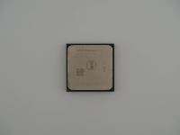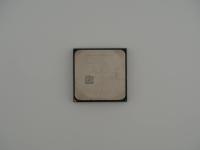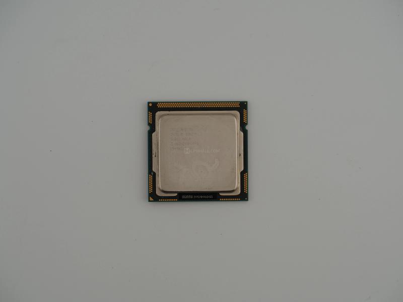
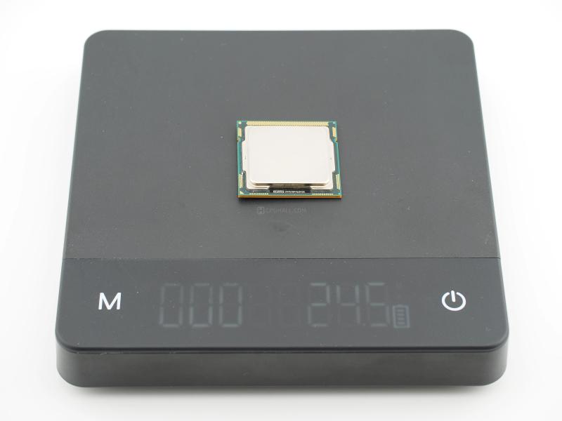
Resting on the digital scale, the chip weighs in at exactly 24.5 grams, a standard mass for modern desktop silicon clad in a copper integrated heat spreader. The nickel plating on the IHS shows minor surface wear from past thermal paste applications, but the laser etching remains razor sharp.
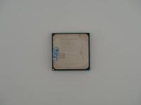
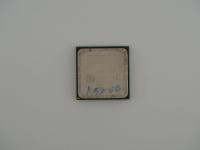
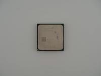
Flipping the artifact over to observe the green organic flip-chip substrate, the central capacitor arrangement is a dead giveaway for Intel's LGA-1156 package. The gold contact pads show faint indentation marks, indicating this chip was securely clamped into a motherboard socket during its operational life.
INTEL (M) (C) '08 i5-750
INTEL (R) CORE (TM) i5
SLBLC MALAY
2.66GHZ/8M/09B
L949B513 (e4)
Substrate PCB Mark: 2V951044A3435
Underneath that protective nickel-plated copper lid lies the Lynnfield core. Built on Intel's highly mature 45nm fabrication node, this die packs approximately 774 million transistors. While the flagship Core i7 parts of the era enjoyed Hyper-Threading, Intel ruthlessly segmented the market by disabling it here, making the i5-750 a strict 4-core, 4-thread processor.
The most fascinating engineering shift represented by this silicon is its integration. Before Lynnfield, motherboards relied heavily on a Northbridge chip to handle memory and graphics communication. With this architecture, Intel dragged the PCI Express root complex directly onto the CPU die itself, providing 16 lanes of PCIe 2.0. Combined with a dual-channel DDR3 memory controller, this drastically simplified motherboard layouts and reduced latency. It communicated with the P55 chipset using the slower DMI interface operating at 2.5 GT/s, bypassing the massive QPI links reserved for the high-end LGA-1366 platform. It was rated for a very manageable 95W Thermal Design Power.
This artifact represents a massive milestone in PC history. It is the very first Core i5. When it dropped in late 2009, it completely redefined the price-to-performance ratio for mainstream computing and gaming.
The lore surrounding the i5-750 is heavily tied to its legendary overclocking headroom. Enthusiasts quickly discovered that by tweaking the Base Clock (BCLK), this 2.66 GHz chip could easily hit 4.0 GHz on air cooling. It was an absolute monster for budget builders. However, this era was not without drama. The aggressive overclocking scene uncovered a physical vulnerability in the hardware ecosystem known as the "Foxconn socket burn" issue. Extreme overclockers pushing massive voltage through the LGA-1156 socket found that poor contact in certain Foxconn-manufactured sockets caused the pins to arc and literally melt the pads on the bottom of the CPU. Fortunately, looking at the pristine pads on this specific unit, it never suffered that fiery fate.
The surface markings on this unit leave zero room for ambiguity. The SLBLC S-Spec code definitively identifies this as the B1 stepping of the Lynnfield desktop processor. Furthermore, the FPO (Finished Process Order) batch code L949B513 provides the exact timeline of its birth.
The "L" designates the manufacturing facility, which aligns with the "MALAY" text indicating assembly in Malaysia. The "9" stands for the year 2009, and "49" represents the 49th week of that year. Therefore, this silicon was packaged in early December 2009, right in the middle of the explosive initial release window for the Nehalem mainstream lineup. It is a perfect, textbook example of the chip that taught a generation of PC gamers how to overclock.