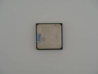
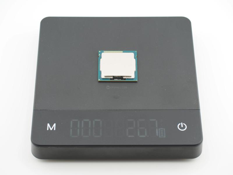
Dropping it on the scale reveals a precise weight of 26.7 grams. Looking under the macro lens at the nickel-plated copper integrated heat spreader (IHS), the laser etching remains remarkably crisp and legible.
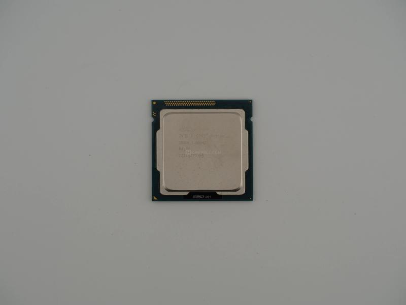
i(M)(C)10
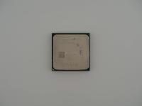
INTEL(R) CORE(TM) i7-3770
SR0PK 3.40GHZ
MALAY
L221B277 (e4)
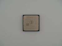
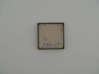
The SR0PK is the crucial S-Spec identifying this as the locked retail or OEM version of the i7-3770. Measuring exactly 37.5mm by 37.5mm against the ruler, the green fiberglass substrate is in great condition. Flipping it over to examine the 1155 gold contact pads reveals zero significant scuffing. The densely packed surface-mount capacitors in the center of the land grid array are characteristic of the Ivy Bridge architectural layout, a stark visual contrast to the layouts seen on the preceding Sandy Bridge generation. It is a highly refined, mass-produced artifact of a pivotal era in semiconductor manufacturing.
This is where the history gets heavy. The Core i7-3770 represents the "tick" in Intel's classic tick-tock development cycle. While the microarchitecture was largely a refinement of the legendary Sandy Bridge, the silicon underneath this IHS was revolutionary. This chip brought 22-nanometer manufacturing to the desktop masses.
More importantly, this was the dawn of 3D Tri-Gate transistors (Intel's marketing term for FinFETs). Before Ivy Bridge, transistors were essentially flat. By raising the transistor channel into a 3D fin shape, Intel engineers drastically reduced power leakage and improved performance at lower voltages. This die contains 1.4 billion transistors crammed into a remarkably small 160 square millimeter footprint. It features four cores, eight threads via Hyper-Threading, 8MB of L3 cache, and it was the first Intel mainstream desktop platform to natively support PCI Express 3.0.
Every heavy metal hero has a controversial album, and Ivy Bridge is no exception. While the i7-3770 was a powerhouse that dominated its AMD FX-series rivals, it sparked one of the most infamous eras in PC hardware lore: the thermal paste controversy.
For generations, high-end Intel desktop chips had their silicon dies soldered directly to the metal IHS using an indium alloy. This provided exceptional heat transfer. With Ivy Bridge, Intel quietly switched to using a standard Thermal Interface Material (TIM), colloquially dubbed "Intel toothpaste" by enraged hardware enthusiasts. Because the 22nm die was so small and dense, heat density spiked. When overclockers pushed the unlocked "K" variants of this architecture, the chips hit thermal walls incredibly fast.
While this specific artifact is the locked S-Spec and not built for extreme overclocking, it shares the exact same physical DNA. The intense heat issues birthed the modern "delidding" craze. Enthusiasts would take razor blades or 3D-printed vices to literally pop the metal lid off these processors, scraping away the factory paste and replacing it with liquid metal to drop temperatures by up to 20 degrees Celsius. Looking at the factory seal still intact on this unit, I am glad it survived the butcher block.
I am absolutely certain of the identification here. The surface markings tell a complete and verified story. The batch code L221B277 breaks down perfectly according to Intel's naming conventions from that era.
The L indicates fabrication in Malaysia, aligning with the "MALAY" text etched right above it. The 2 dictates the year of manufacture as 2012. The 21 tells us it rolled off the assembly line during the 21st week of that year. The (e4) in the corner signifies the chip is lead-free and RoHS compliant, a standard marking for consumer electronics of the 2010s. This specific unit was manufactured right at the height of the Ivy Bridge launch window, hitting shelves to upgrade LGA-1155 motherboards worldwide. It is a perfect, pristine textbook example of the architecture that bridged the gap between raw clock speed wars and modern efficiency.