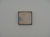
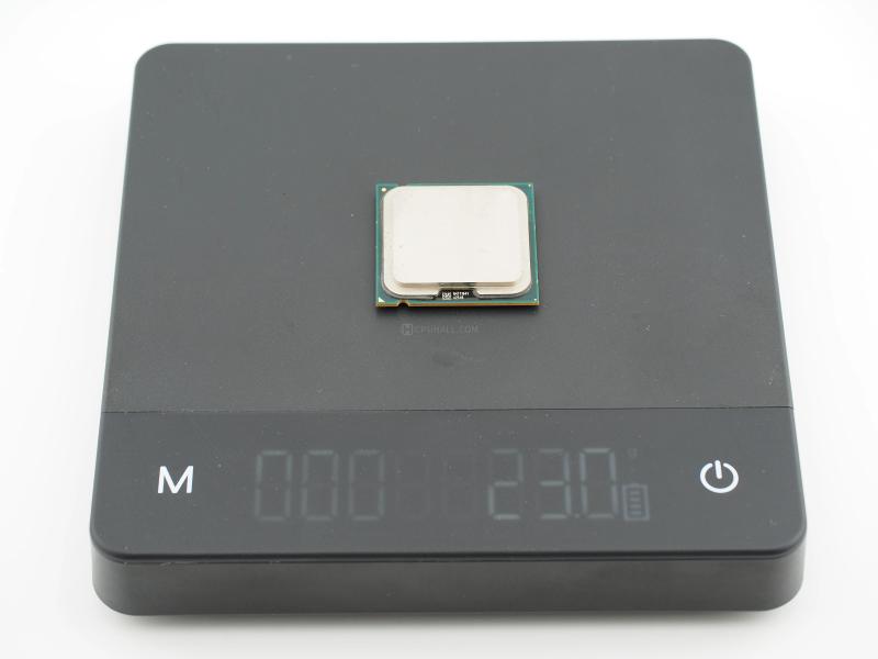
Placing it on the scale yields a solid 23.0 grams, almost entirely dominated by the thick nickel-plated copper Integrated Heat Spreader (IHS) designed to tame the fiery NetBurst architecture beneath.
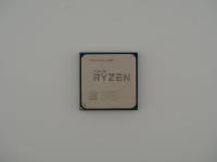
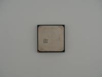
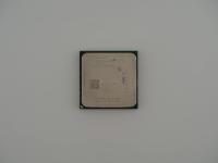
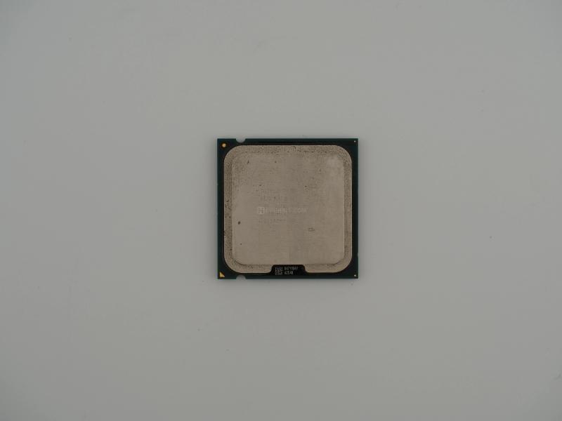
Looking closely at the surface under bright light, the laser etching is remarkably pristine. The text gives us a perfect snapshot of the era:
INTEL (m)(c) '06
PENTIUM(R) 4
631 SL9KG MALAY
3.00GHZ/2M/800/06
L712A752 (e4)
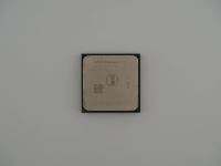
Flipping this piece over reveals the LGA-775 contact pads, a beautiful grid of gold that marked Intel's permanent transition away from delicate pins on the CPU itself. The central array of surface-mounted capacitors is arranged in a dense grid, characteristic of the late-stage Pentium 4 packages. The PCB substrate feels rigid and utilitarian, entirely typical for high-volume consumer silicon of the mid-2000s. There are some slight scuffs on the heat spreader wings where the socket retention mechanism clamped down over the years, a distinct footprint of its operational life.
To understand the engineering of this chip, we have to talk about Cedar Mill. This was Intel's 65-nanometer die shrink of the infamous Prescott core. By moving to a 65nm fabrication process, Intel managed to pack 188 million transistors into a die size of just 81 square millimeters.
The underlying NetBurst architecture was a fascinating, if ultimately flawed, approach to compute performance. It utilized a ridiculously deep 31-stage pipeline. The engineering philosophy was simple: sacrifice instructions per clock (IPC) to push clock speeds to the absolute moon.
This specific chip runs at a base clock of 3.00 GHz with an 800 MHz Front Side Bus (FSB) and features a massive (for the time) 2MB of L2 cache. The 06 in the part number refers to the Platform Compatibility Guide (PCG), ensuring motherboard voltage regulators could handle its 86-watt Thermal Design Power (TDP). While 86W seems modest by today's server standards, trying to dissipate that heat through a small die area on consumer air coolers in 2006 was a significant thermal challenge.
This processor represents the twilight of the NetBurst era. For years, Intel engineers boldly claimed that NetBurst would scale to 10 GHz. Reality hit them like a brick wall in the form of leakage current and thermal limits. The preceding Prescott cores ran so hot they became industry-wide jokes, earning nicknames like "PresHot" and spawning memes about using PCs as winter space heaters.
However, the Cedar Mill core inside this Pentium 4 631 is actually a legendary piece of silicon among a very specific group of enthusiasts: extreme overclockers. Because the 65nm process significantly reduced the heat and voltage requirements compared to Prescott, these chips had an insane amount of thermal headroom. On standard air cooling, a 631 could easily be pushed past 4.5 GHz. Under liquid nitrogen, the NetBurst 10 GHz dream almost became a reality, with extreme overclockers pushing these specific 65nm Pentium 4s beyond 8 GHz. It is a chip that failed its original architectural destiny but accidentally became a holy grail for voltage junkies.
Reading the batch code on this specific unit tells a very clear story of its origin. The FPO code L712A752 breaks down perfectly. The "L" indicates it was fabbed and packaged in Malaysia. The "7" reveals the year of manufacture is 2007, specifically the 12th week of the year.
This date is historically fascinating. By early 2007, Intel's Core 2 Duo (Conroe) had already launched and utterly destroyed NetBurst in both performance and efficiency. Yet, Intel was still churning out these Pentium 4 chips to satisfy budget desktop markets and OEM contracts.
Furthermore, the S-Spec SL9KG confirms this is the highly refined D0 stepping. The D0 stepping was the absolute final optimization of the Cedar Mill core, dropping the TDP from 86W down to a much more manageable 65W in later revisions, although the IHS markings often retained the older PCG ratings. This chip represents the absolute final, most polished form of an architecture that Intel was actively trying to forget.